Monolithic ceramic electronic component

a technology of electronic components and monolithic ceramics, applied in the direction of fixed capacitor details, stacked capacitors, fixed capacitors, etc., can solve the problems of large thickness of outer electrodes formed by this method, which is a few tens to several hundreds of micrometers thick, and achieves the effect of reducing the thickness of outer electrodes

Active Publication Date: 2014-10-02
MURATA MFG CO LTD
View PDF4 Cites 13 Cited by
  • Summary
  • Abstract
  • Description
  • Claims
  • Application Information

AI Technical Summary

Benefits of technology

[0007]Accordingly, preferred embodiments of the present invention provide a monolithic ceramic electronic component in which a force fixing an outer electrode to a component body, the outer electrode including a plating film that is directly connected to electrode layers such as inner electrodes, is significantly increased.
[0014]The electrode layers preferably include an inner electrode arranged along an interface between the ceramic layers, and a surface electrode arranged along the ceramic layers and on an outer surface of the component body. With this structure, the area of the exposed portion distribution region is significantly increased. Consequently, the outer electrode is provided over a wider surface on the component body, and the force with which the outer electrode is fixed to the component body is further increased.
[0015]According to a preferred embodiment of the present invention, the first plating layer preferably includes a Ni—P plating layer, and a phosphorus content of the first plating layer is preferably about 9% by weight to about 13% by weight, for example. With this structure, the force with which the outer electrode is fixed is further increased. Furthermore, this structure also contributes to the improvement in thermal shock resistance and moisture-proof reliability.
[0017]According to a preferred embodiment of the present invention, it is possible to increase the force with which an outer electrode is fixed to a component body, the outer electrode including a plating film that is directly connected to electrode layers.
[0019]On the other hand, the second plating layer formed so as to cover the first plating layer is formed by electrolytic plating. In electrolytic plating, plating is grown faster than in electroless plating. Accordingly, a plating film formed by electrolytic plating strongly engages with irregularities on a ceramic surface compared with a plating film formed by electroless plating. Therefore, an electrolytic plating film achieves a larger anchoring effect on the ceramic surface, and consequently, a higher joining force is realized.

Problems solved by technology

However, an outer electrode formed by this method has a large thickness of several tens to several hundreds of micrometers.
However, the outer electrode formed by this method has the following problem.

Method used


Image

  • Monolithic ceramic electronic component
  • Monolithic ceramic electronic component
  • Monolithic ceramic electronic component

Examples


first preferred embodiment

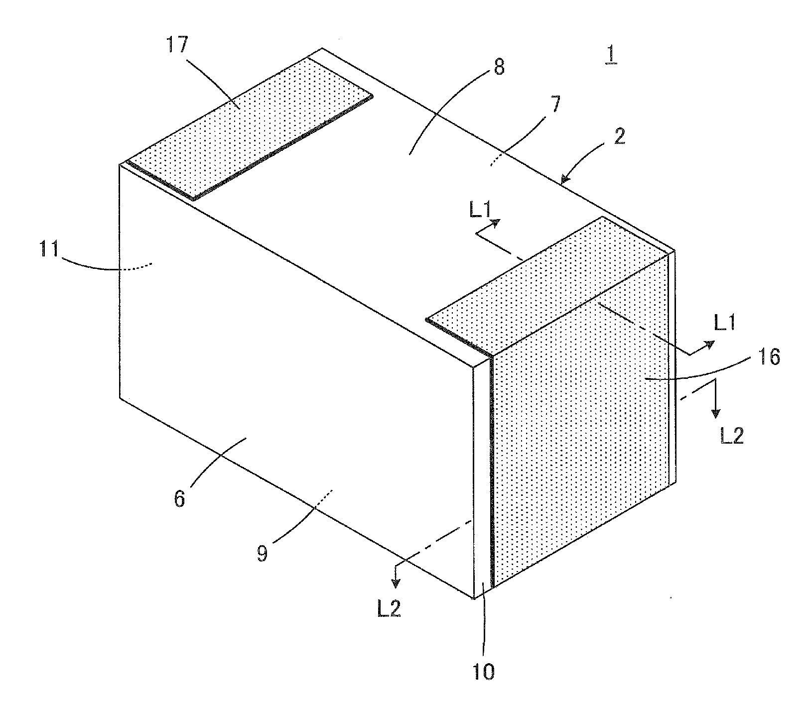
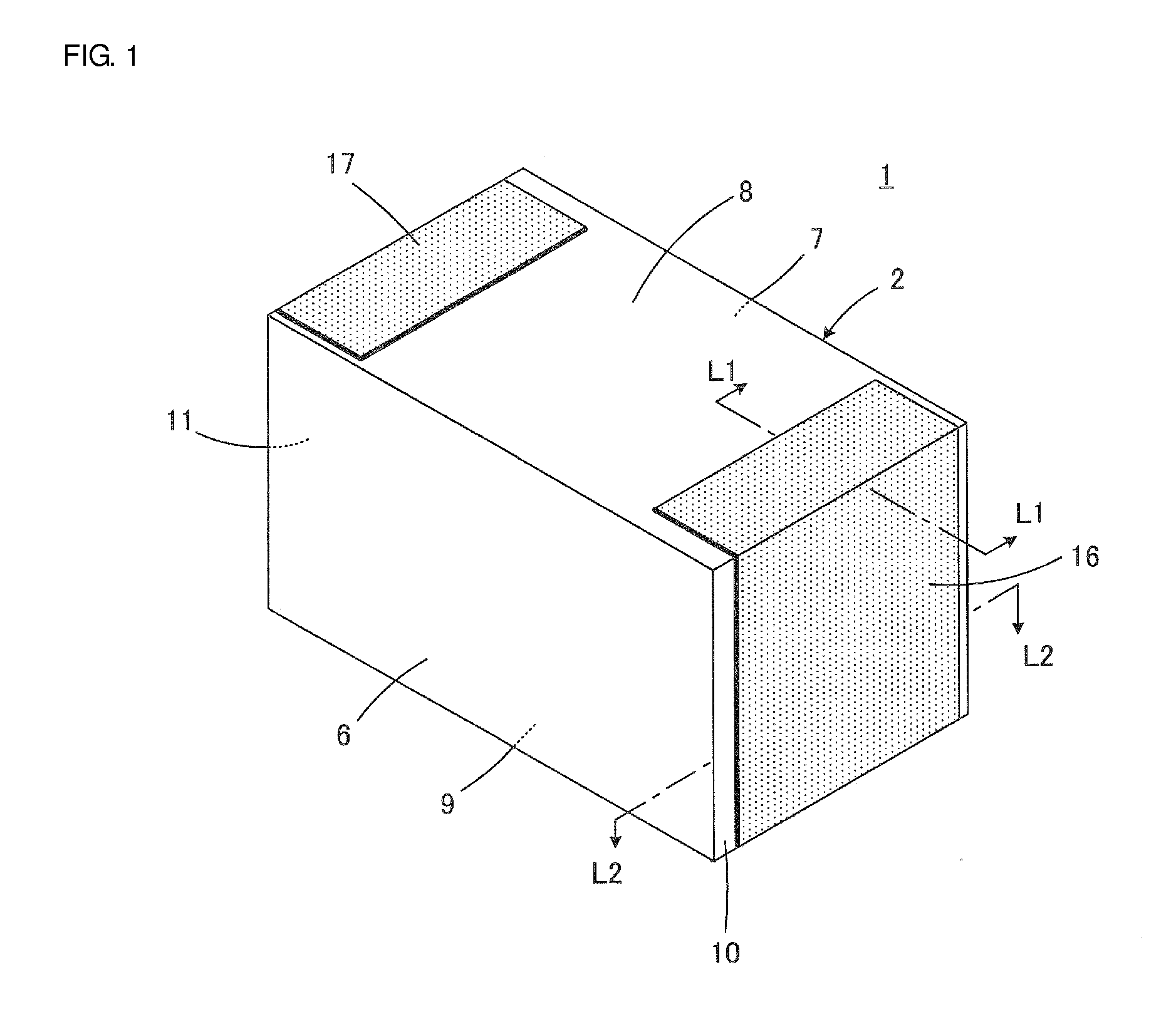
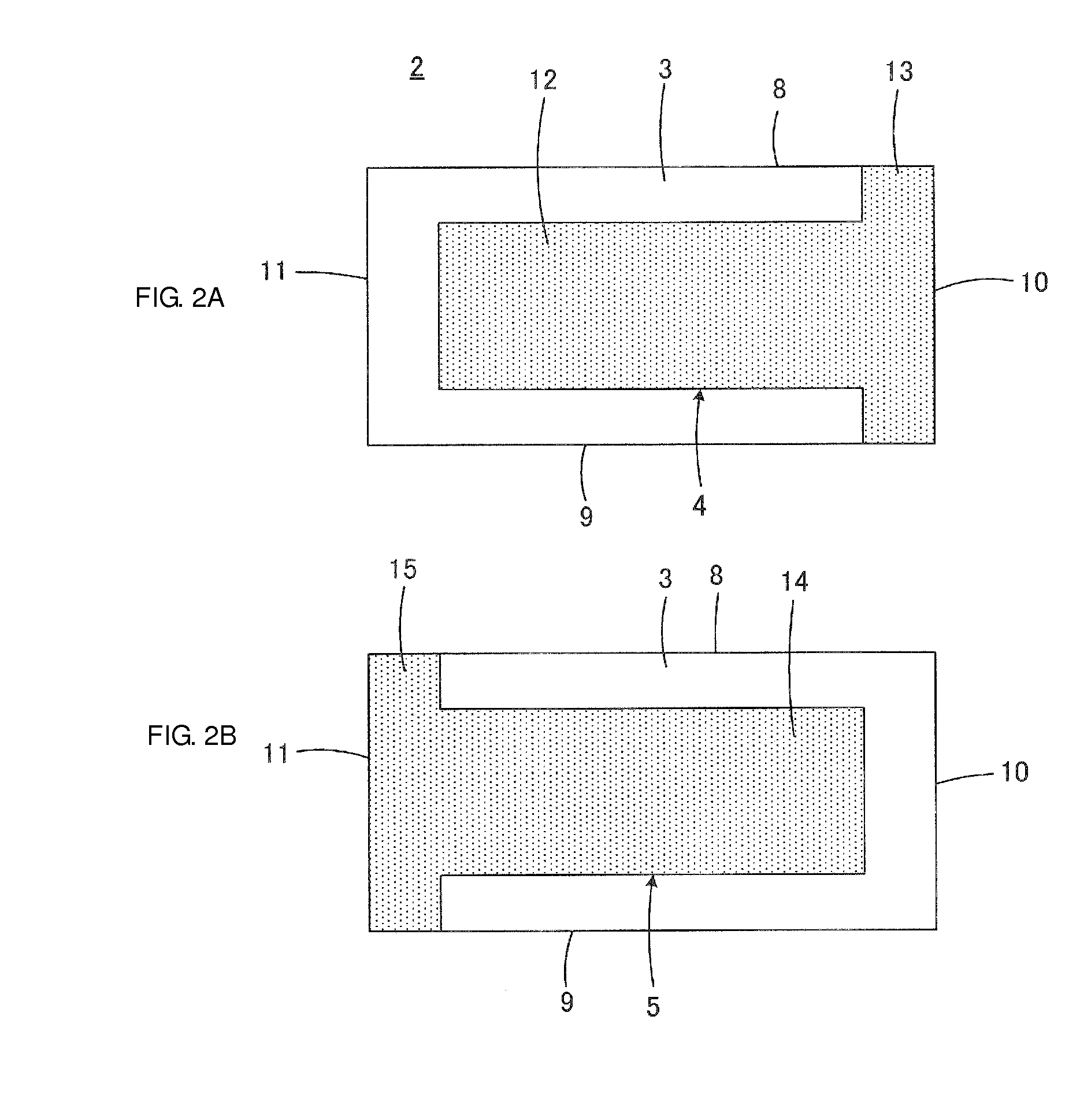
[0040]FIGS. 1 to 5 are views illustrating a two-terminal-type monolithic ceramic capacitor 1 according to a first preferred embodiment of the present invention. The monolithic ceramic capacitor 1 includes a component body 2 whose appearance is shown in FIG. 3. The component body 2 includes a plurality of stacked ceramic layers 3, and first inner electrodes 4 and second inner electrodes 5 that serve as a plurality of electrode layers arranged along the ceramic layers 3. The inner electrodes 4 and 5 are disposed at interfaces between the ceramic layers 3. The ceramic layers 3 preferably are composed of, for example, a barium titanate-based dielectric ceramic. The inner electrodes 4 and 5 preferably contain, for example, Ni as a conductive component.

[0041]The component body 2 has a rectangular or substantially rectangular parallelepiped shape including a first main surface 6 and a second main surface 7 that extend in a direction in which the ceramic layers 3 extend, a first lateral sur...

experimental example 1

[0077]A component body for a monolithic ceramic capacitor was prepared. The component body had a planar dimension of approximately 1.0 mm×0.5 mm, and included ceramic layers composed of a barium titanate-based dielectric ceramic and inner electrodes containing Ni as a main component. In this component body, the ceramic layers between the inner electrodes each had a thickness of about 1 μm, each of the inner electrodes had a thickness of about 1 μm, and outer layer portions that did not include the inner electrodes each had a thickness of about 50 μm, for example. As a pretreatment of a plating process described below, barrel polishing was performed on the component body so that exposed portions of the inner electrodes were reliably exposed. Subsequently, a washing step with pure water was performed.

[0078]Next, a step of imparting a Pd catalyst was performed for the component body. In the step of imparting a Pd catalyst, an aqueous solution of palladium chloride (Pd concentration: 10...

experimental example 2

[0085]A component body for a monolithic ceramic capacitor was prepared. The component body had a planar dimension of approximately 0.6 mm×0.3 mm and included ceramic layers composed of a barium titanate-based dielectric ceramic and inner electrodes containing Ni as a main component. In this component body, the ceramic layers between the inner electrodes each had a thickness of about 1 μm, each of the inner electrodes had a thickness of about 0.7 μm, and outer layer portions that did not include the inner electrodes each had a thickness of about 50 μm.

[0086]A first plating layer constituted by a Ni—P plating film having a P content of about 11% by weight was formed on the component body through the steps similar to those in Experimental Example 1. Here, the distance from an edge of the exposed portion distribution region to an edge of the first plating layer, that is, the amount of extension of first plating was changed by varying the electroless plating process time for forming the ...


PUM

PropertyMeasurementUnit
distanceaaaaaaaaaa
thicknessaaaaaaaaaa
dielectricaaaaaaaaaa

Abstract

A monolithic ceramic electronic component includes an outer electrode including a first plating layer formed directly on a component body by electroless plating so as to cover an exposed portion distribution region including exposed portions of a plurality of inner electrodes and a second plating layer formed by electrolytic plating so as to cover the first plating layer. An amount of extension of the first plating E1 and an amount of extension of the second plating E2 satisfy the relationship E1 / (E1+E2)≦20%, where E1 represents a distance from an edge of the exposed portion distribution region to an edge of the first plating layer, and E2 represents a distance from the edge of the first plating layer to an edge of the second plating layer.

Description

BACKGROUND OF THE INVENTION[0001]1. Field of the Invention[0002]The present invention relates to a monolithic ceramic electronic component, in particular, to a monolithic ceramic electronic component in which an outer electrode that is connected to electrode layers such as inner electrodes located along ceramic layers includes a plating film and the plating film is directly connected the electrode layers.[0003]2. Description of the Related Art[0004]An outer electrode of a monolithic ceramic capacitor, which is an example of a monolithic ceramic electronic component, is usually formed by applying a conductive paste onto an end portion of a component body, and baking the conductive paste. However, an outer electrode formed by this method has a large thickness of several tens to several hundreds of micrometers. Accordingly, in order to control the dimensions of such a monolithic ceramic capacitor so as to be within certain specified values, it is necessary to undesirably reduce the eff...

Claims


Application Information

Patent Timeline
Patent Type & Authority Applications(United States)
IPC IPC(8): H01G4/005H01G4/008H01G4/30
CPCH01G4/005H01G4/008H01G4/30H01C1/148H01C7/008H01C7/18H01F17/0013H01G4/012H01G4/232H01G4/2325H01F27/292H10N30/872H10N30/871
Inventor SASABAYASHI, TAKEHISAMOTOKI, AKIHIROOGAWA, MAKOTO
Owner MURATA MFG CO LTD
Why Eureka
Try Eureka