Single cell array microchip and fabrication, electrical measurement and electroporation method thereof
a single cell array and microchip technology, applied in the field of biodetection technologies, can solve the problems of difficult to compliment efficiency and precision of measurement, limited function to one single purpose, complicated operation process, etc., and achieve the effects of reducing cell mortality rate, improving efficiency of electroporation, and effective improvement of cell electrical measuremen
- Summary
- Abstract
- Description
- Claims
- Application Information
AI Technical Summary
Benefits of technology
Problems solved by technology
Method used
Image
Examples
example 1
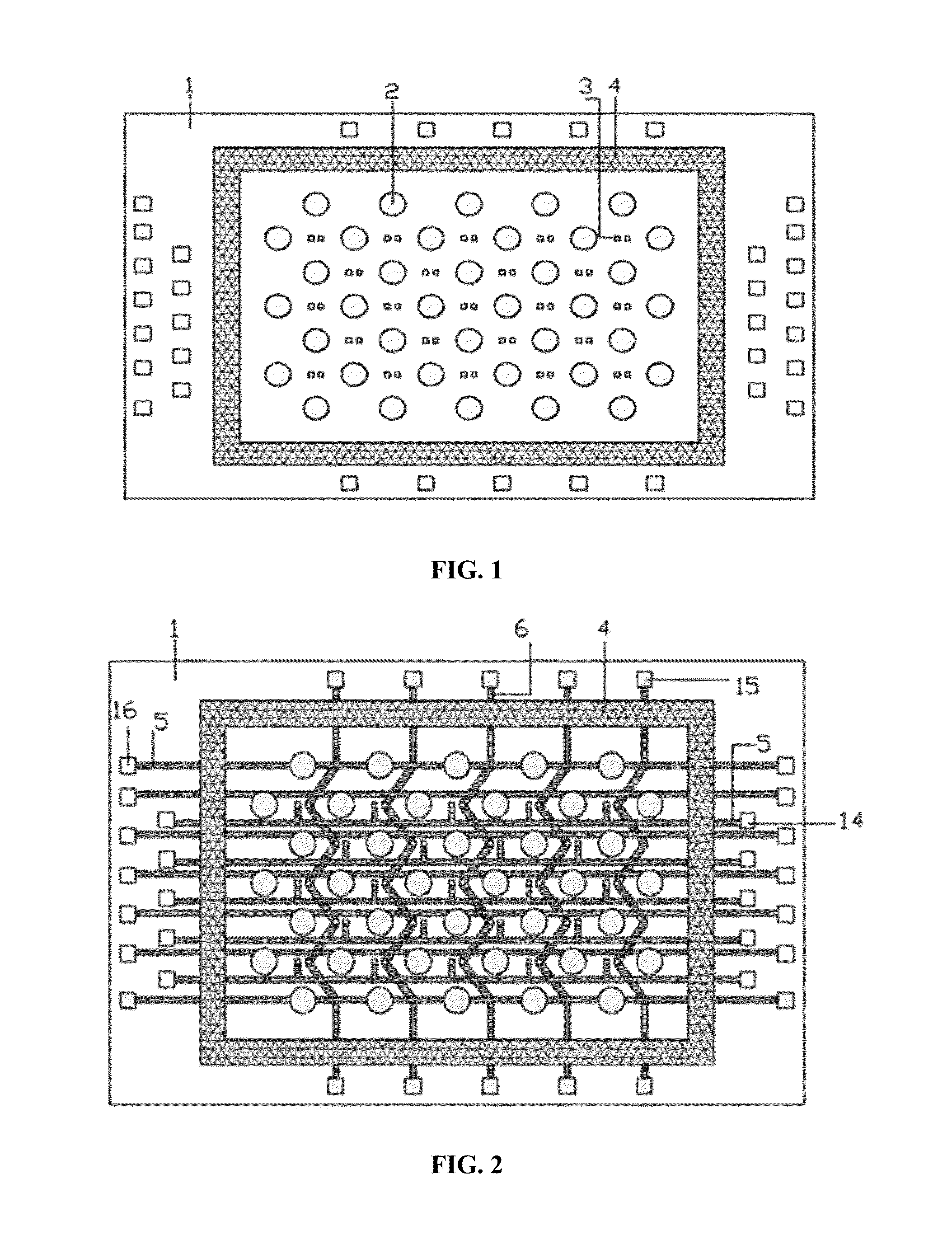
[0040]As is illustrated in FIG. 1 and FIG. 2, the present invention provides a single cell array microchip, comprising a substrate 1; a plurality of positioning electrodes which form an array 2; an array of measuring electrode-pairs 3; a micro sample pool 4. Each four adjacent positioning electrodes 2 form a shape of a rhombus functioning as one positioning unit. At the centre of the recited positioning unit lies a pair of measuring electrodes 3. Each row of the multiple positioning electrodes 2 are connected by lateral bars 5. Two electrodes in each measuring electrode pair 3 are connected with an electrode in an adjacent measuring electrode pair by the longitudinal bar 6 and the lateral bar 5 respectively.
[0041]The lateral bars 5 and the longitudinal bars 6 are patterned in different layers with an insulating layer in between.
[0042]The substrate 1 is made of an insulating material, such as glass, or silicon covered with an insulating layer. The micro sample pool 4 is constructed w...
example 2
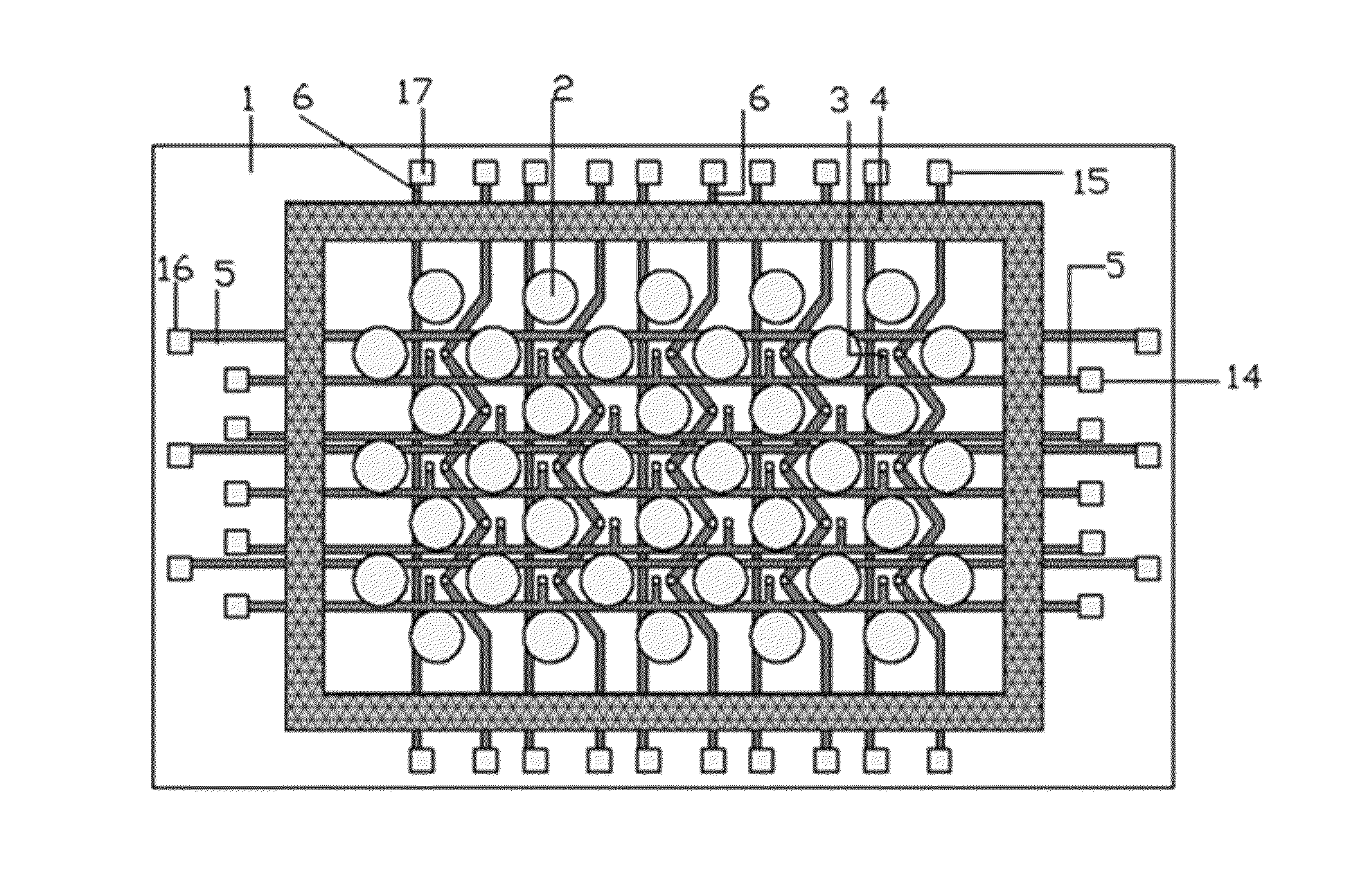
[0043]FIG. 3 shows another embodiment of the present invention which is different from embodiment 1 in the layout of the connecting bars of the positioning electrodes 2. As can be seen from the drawing, the two pairs of the opposite electrodes in each positioning unit are connected with other positioning electrodes in adjacent positioning unit by longitudinal 6 and lateral bars 5 respectively. For the lateral bars of positioning electrodes, the electrical signal is inputted and outputted via the bonding pad 16, and for the longitudinal bars of positioning electrodes, the electrical signal is inputted and outputted via the bonding pad 17.
example 3
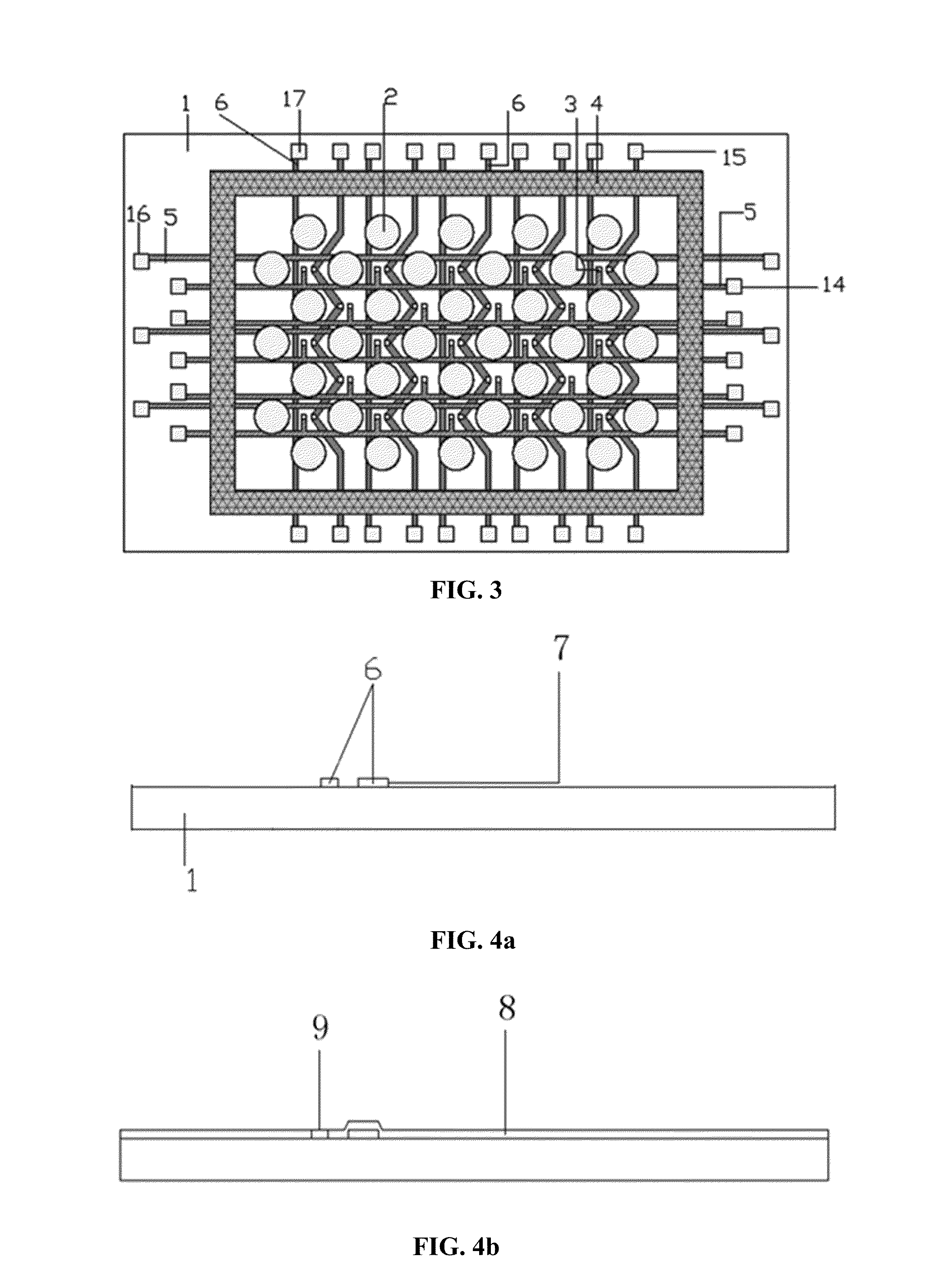
[0044]FIGS. 4a-4f illustrate the fabrication process of single cell array microchip according to one aspect of the present invention. A glass substrate is employed to fulfill the fabrication with the following steps orderly.
[0045]a. The first layer of Ti / Au 7 is sputtered on the glass substrate 1, followed by the lithography process to pattern the longitudinal electrode bars 6.
[0046]b. The first insulating layer of SiO2 8 is deposited and etched to open the window of electrodes (and the bonding pads) 9.
[0047]c. The second layer of Ti / Au 10 is deposited, followed by the lithography process to pattern the lateral electrode bars 5.
[0048]d. The second insulating layer of SiO2 11 is deposited and etched to open the window of electrodes (and the bonding pads) 12.
[0049]e. The third layer of Ti / Au 13 is deposited, followed by the lithography process to pattern the positioning electrodes 2 and the measuring electrode-pairs 3 and bonding pads 14, 15, 16, 17.
[0050]f. The micro sample pool 4 is...
PUM
| Property | Measurement | Unit |
|---|---|---|
| shape | aaaaa | aaaaa |
| insulating | aaaaa | aaaaa |
| electrical | aaaaa | aaaaa |
Abstract
Description
Claims
Application Information


