Via Fill Material For Solar Applications

a solar cell and filling material technology, applied in the direction of printed element electric connection formation, semiconductor/solid-state device details, conductors, etc., can solve the problems of low shunt resistance and particularly difficult solar cell parasitic resistance management, and achieve excellent shunt performance

Inactive Publication Date: 2014-11-13
HERAEUS PRECIOUS METALS NORTH AMERICA CONSHOHOCKEN
View PDF3 Cites 14 Cited by
  • Summary
  • Abstract
  • Description
  • Claims
  • Application Information

AI Technical Summary

Benefits of technology

[0011]There are three main features of the invention. The first feature deals with control of sintering during the firing process. This is achieved through careful selection of metal powders with certain particle size, use of glasses with certain melting point and oxides which affect the sintering behavior. The second feature relates to shunting behavior. Excellent shunt performance is achieved by controlling reaction between via-fill paste and the surrounding hole. This is controlled through selection of glass and proportions of oxides. The third feature is related to solderability and adhesion of the fired film. This is achieved by selection of glass having reactivity towards silicon wafer and selection of metal powder which during the sintering process does not squeeze glass to the surface. In addition to the above the paste rheology is controlled to achieve good via filling through selection of organic resin.

Problems solved by technology

The formation of an electrically conductive pathway through a via presents a particularly difficult problem in terms of managing parasitic resistance in a solar cell.
But because the via fill material contacts the silicon wafer within the via, the via fill material can also form an electrically conductive path (shunt) across the P-N junction, disadvantageously leading to low shunt resistance.

Method used


Image

  • Via Fill Material For Solar Applications
  • Via Fill Material For Solar Applications
  • Via Fill Material For Solar Applications

Examples


examples

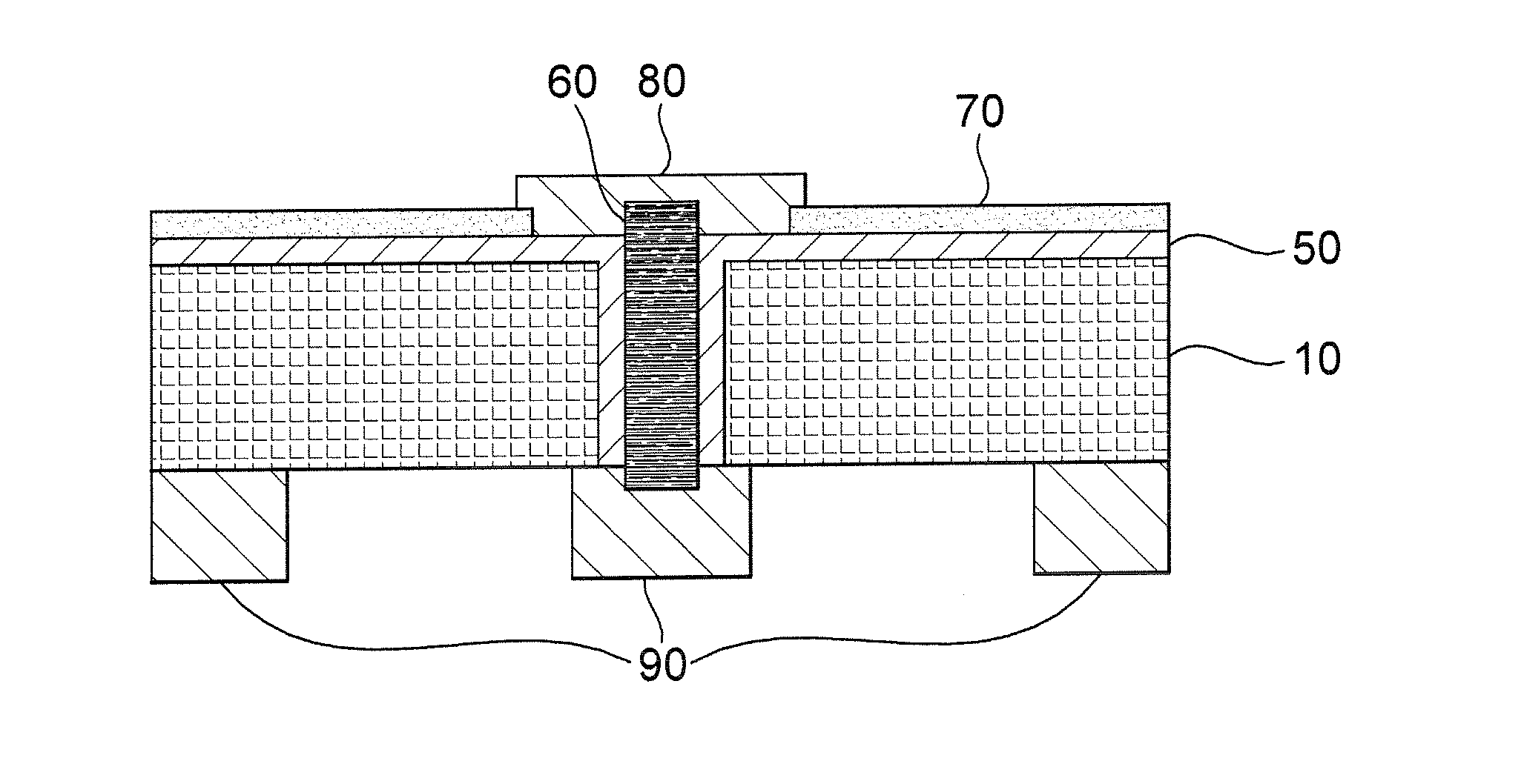
[0038]Polycrystalline silicon wafers, 12.5 cm×12.5 cm, thickness 250-300 μm, were coated with a silicon nitride antireflective coating on the N-side of the wafer. The sheet resistivity of these wafers was about 1 Ω-cm. A contact grid was formed on the antireflective coating using Ferro NS33-502 and NS33-503 pastes, commercially available from Ferro Corporation, Vista, Calif., by screen printing.

[0039]Vias on the order of 200 microns in diameter were formed through the wafers using laser drilling before diffusion process.

[0040]Two glass frits were separately produced using conventional glass making techniques so as to achieve a composition shown in parts by weight in Table 2:

TABLE 2Glass Compositions in weight %12PbO28.956.1ZnO—19.6SiO2—14.4Al2O3—6.6P2O512.3—V2O558.8—Ta2O5—3.3

[0041]Each of the glass frits was separately milled to a fineness of 2 to 5 microns D50. Three via fill material compositions according to the invention were prepared by blending the components listed in parts b...


PUM

PropertyMeasurementUnit
wt %aaaaaaaaaa
D50 sizesaaaaaaaaaa
D50 particle sizeaaaaaaaaaa

Abstract

The present invention is directed toward a via fill material for use in solar applications that exhibits low series resistance and high shunt resistance. The via fill material according to the invention includes silver powder, a glass frit and a vehicle.

Description

BACKGROUND OF THE INVENTION[0001]1. Field of Invention[0002]The present invention relates to a via fill material for use in solar applications that exhibits low series resistance and high shunt resistance. This new solar cell structure is a back contact solar cell device. In this device the contacts to the p and n surfaces are made on the backside of the solar cell. Such structures have advantages in terms of reducing shadow losses and hence increasing solar efficiency. This invention particularly deals with a key metallization which connects the front side of the solar cell to the backside through a hole as shown in FIG. 1.[0003]2. Description of Related Art[0004]Solar cells, which are also sometimes referred to in the art as photovoltaic cells, convert solar energy into electricity by means of the photoelectric effect. The most commonly known solar cells comprise large-area P-N junction devices. Such solar cells typically comprise a silicon wafer that has been doped on an N-side w...

Claims


Application Information

Patent Timeline
Patent Type & Authority Applications(United States)
IPC IPC(8): H01L31/0224H05K3/42
CPCH01L31/022425H05K3/42H05K2203/1126C03C3/07C03C3/16C03C8/10C03C8/18C03C8/20H01B1/22H01L23/481H01L31/02245H01L2924/0002Y02E10/50Y10T29/49165H01L2924/00H01B1/16H01L31/042
Inventor GRADDY, JR., GEORGE E.MCKINLEY, CAROLINE M.SHAIKH, AZIZ S.
Owner HERAEUS PRECIOUS METALS NORTH AMERICA CONSHOHOCKEN
Why Eureka
Try Eureka