Semiconductor device

a technology of semiconductors and on-state currents, applied in semiconductor devices, electrical devices, transistors, etc., can solve the problems of difficult to achieve sufficient high on-state current, deterioration of electric characteristics, etc., and achieve low power consumption, high degree of integration, and reduced deterioration of on-state current characteristics

Inactive Publication Date: 2014-11-20
SEMICON ENERGY LAB CO LTD
View PDF10 Cites 77 Cited by
  • Summary
  • Abstract
  • Description
  • Claims
  • Application Information

AI Technical Summary

Benefits of technology

[0013]One object of one embodiment of the present invention is to provide a semiconductor device in which deterioration of electric characteristics which becomes more noticeable as the semiconductor device is miniaturized can be suppressed. Another object is to provide a semiconductor device having a high degree of integration. Another object is to provide a semiconductor device in which deterioration of on-state current characteristics is reduced. Another object is to provide a semiconductor device with low power consumption. Another object is to provide a semiconductor device with high reliability. Another object is to provide a semiconductor device which can retain data even when power supply is stopped. Another object is to provide a novel semiconductor device.

Problems solved by technology

However, it is known that miniaturization of a transistor causes deterioration of electric characteristics, such as on-state current, threshold voltage, and an S value (subthreshold value), of the transistor.
In that case, however, a surface area where a channel is formed is increased, which increases carriers scattering at an interface between a channel formation region and a gate insulating film; thus, achieving sufficiently high on-state current is not easy.

Method used


Image

  • Semiconductor device
  • Semiconductor device
  • Semiconductor device

Examples


embodiment 1

[0067]In this embodiment, a semiconductor device of one embodiment of the present invention is described with reference to drawings.

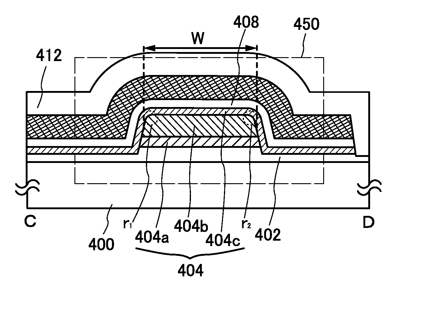
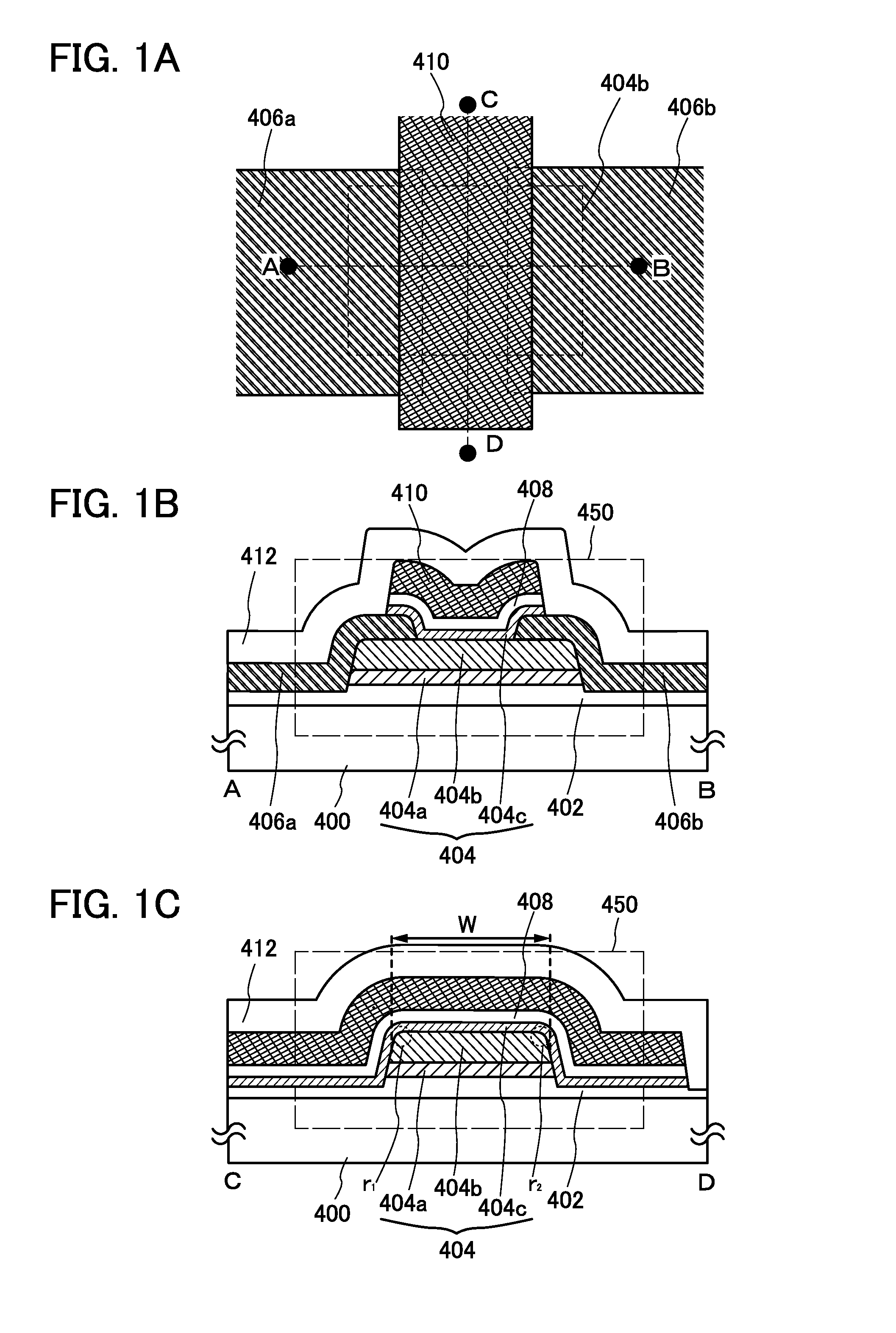
[0068]FIGS. 1A to 1C are a top view and cross-sectional views which illustrate a transistor of one embodiment of the present invention. FIG. 1A is the top view. FIG. 1B illustrates a cross section taken along the dashed-dotted line A-B in FIG. 1A. FIG. 1C illustrates a cross section taken along the dashed-dotted line C-D in FIG. 1A. Note that for simplification of the drawing, some components are not illustrated in the top view in FIG. 1A. In some cases, the direction of the dashed-dotted line A-B is referred to as a channel length direction, and the direction of the dashed-dotted line C-D is referred to as a channel width direction. Note that the channel length is a length of a channel formation region in the direction in which carriers flow. The channel width is a length of the channel formation region, which is perpendicular to the channel length dir...

embodiment 2

[0142]In this embodiment, a method for forming the transistor 450, which is described in Embodiment 1 with reference to FIGS. 1A to 1C, is described with reference to FIGS. 8A to 8C and FIGS. 9A to 9C.

[0143]First, the base insulating film 402 is formed over the substrate 400 (see FIG. 8A).

[0144]For the substrate 400, a glass substrate, a ceramic substrate, a quartz substrate, a sapphire substrate, or the like can be used. Alternatively, a single crystal semiconductor substrate or a polycrystalline semiconductor substrate made of silicon, silicon carbide, or the like, a compound semiconductor substrate made of silicon germanium or the like, a silicon-on-insulator (SOI) substrate, or the like can be used. Further alternatively, any of these substrates further provided with a semiconductor element can be used.

[0145]The base insulating film 402 can be formed by a plasma CVD method, a sputtering method, or the like using an oxide insulating film of aluminum oxide, magnesium oxide, silico...

embodiment 3

[0232]In this embodiment, a transistor having a structure different from that of the transistor described in Embodiment 1 is described.

[0233]FIGS. 14A, 14B, and 14C are a top view and cross-sectional views of a transistor of one embodiment of the present invention. FIG. 14A is the top view, FIG. 14B is a cross section taken along the dashed-dotted line A-B in FIG. 14A, and FIG. 14C is a cross section taken along the dashed-dotted line C-D in FIG. 14A. Note that for simplification of the drawing, some components are not illustrated in the top view of FIG. 14A. The dashed-dotted line A-B direction is referred to as a channel length direction and the dashed-dotted line C-D direction is referred to as a channel width direction, in some cases.

[0234]A transistor 550 illustrated in FIGS. 14A to 14C includes the base insulating film 402 over the substrate 400; the first oxide film 404a and the oxide semiconductor film 404b over the base insulating film 402; the source electrode 406a and the...


PUM


Abstract

Provided is a semiconductor device in which deterioration of electric characteristics which becomes more noticeable as the semiconductor device is miniaturized can be suppressed. The semiconductor device includes a first oxide film, an oxide semiconductor film over the first oxide film, a source electrode and a drain electrode in contact with the oxide semiconductor film, a second oxide film over the oxide semiconductor film, the source electrode, and the drain electrode, a gate insulating film over the second oxide film, and a gate electrode in contact with the gate insulating film. A top end portion of the oxide semiconductor film is curved when seen in a channel width direction.

Description

TECHNICAL FIELD[0001]The present invention relates to a semiconductor device.[0002]In this specification, a “semiconductor device” refers to a device that can function by utilizing semiconductor characteristics; an electro-optical device, a semiconductor circuit, and an electronic device are all included in the category of the semiconductor device.BACKGROUND ART[0003]Attention has been focused on a technique for forming a transistor using a semiconductor thin film formed over a substrate having an insulating surface. The transistor is used in a wide range of electronic devices such as an integrated circuit (IC) and an image display device (display device). A silicon-based semiconductor material is widely known as a material for a semiconductor thin film applicable to a transistor. As another example, an oxide semiconductor has been attracting attention.[0004]For example, a transistor whose active layer includes an amorphous oxide semiconductor containing indium (In), gallium (Ga), a...

Claims


Application Information

Patent Timeline
Patent Type & Authority Applications(United States)
IPC IPC(8): H01L29/786
CPCH01L29/7869H01L29/785H01L29/7854H01L29/78696H01L27/1225H01L29/41733
Inventor HANAOKA, KAZUYAMATSUBAYASHI, DAISUKEKOBAYASHI, YOSHIYUKIYAMAZAKI, SHUNPEIMATSUDA, SHINPEI
Owner SEMICON ENERGY LAB CO LTD
Why Eureka
Try Eureka