A planar optical component and its design method

Inactive Publication Date: 2014-11-20
CAPITAL NORMAL UNIVERSITY
View PDF4 Cites 10 Cited by
  • Summary
  • Abstract
  • Description
  • Claims
  • Application Information

AI Technical Summary

Benefits of technology

The present invention is designed to achieve desired beam shaping effects using a specific structure of an optical component called a planar diffractive optical component. This is achieved by modulating the structural parameter of the component and the amplitude and phase of the radiation field with specific wavelength and polarization states. The planar diffractive optical component is designed to have little difference from its expected parameters, making it an effective solution for achieving optimal beam shaping effects.

Problems solved by technology

Currently, it's only limited applications that phase discontinuity is applied for beam shaping, let alone in the design of optical components.

Method used


Image

  • A planar optical component and its design method
  • A planar optical component and its design method
  • A planar optical component and its design method

Examples


embodiment 1

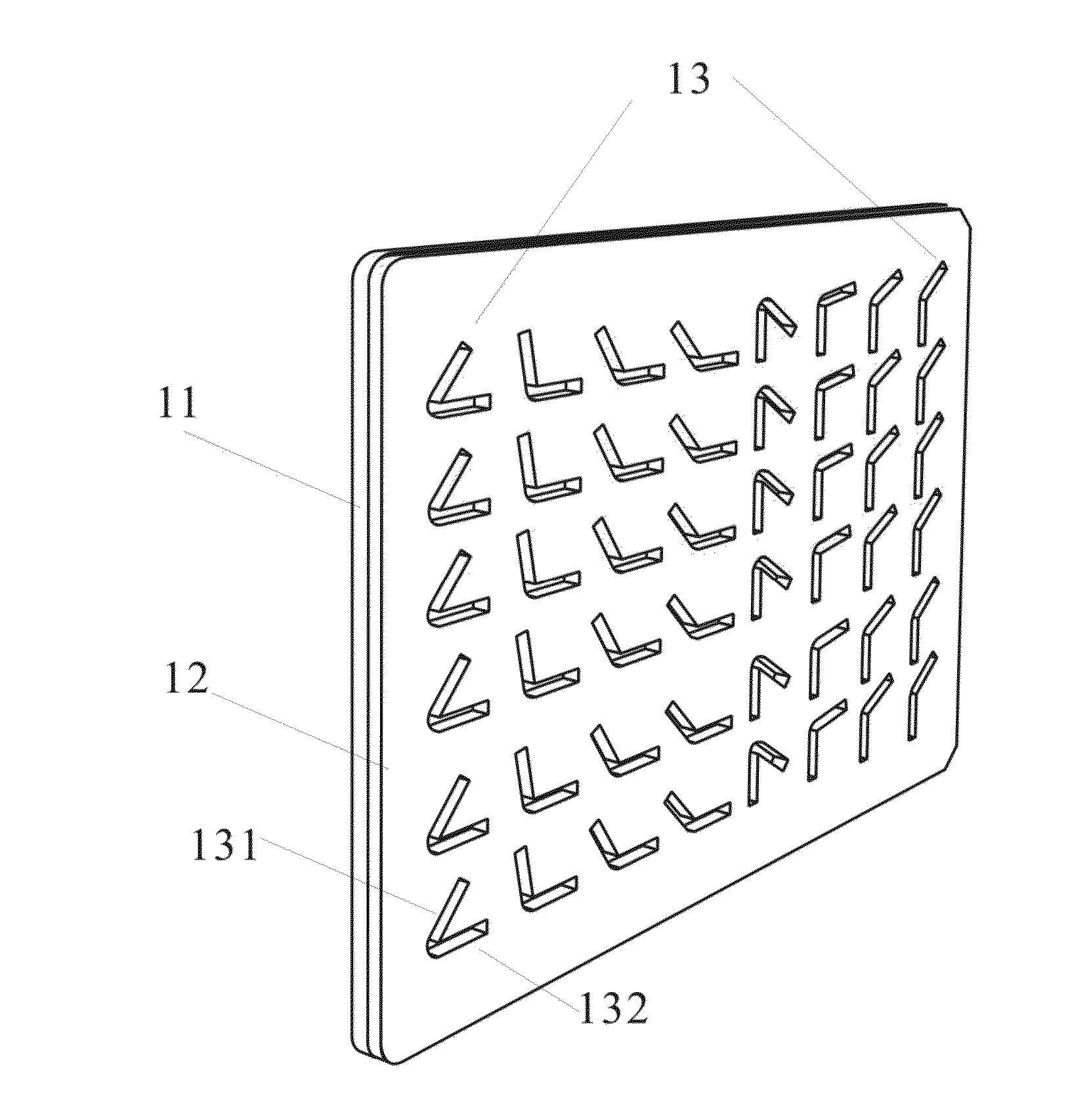
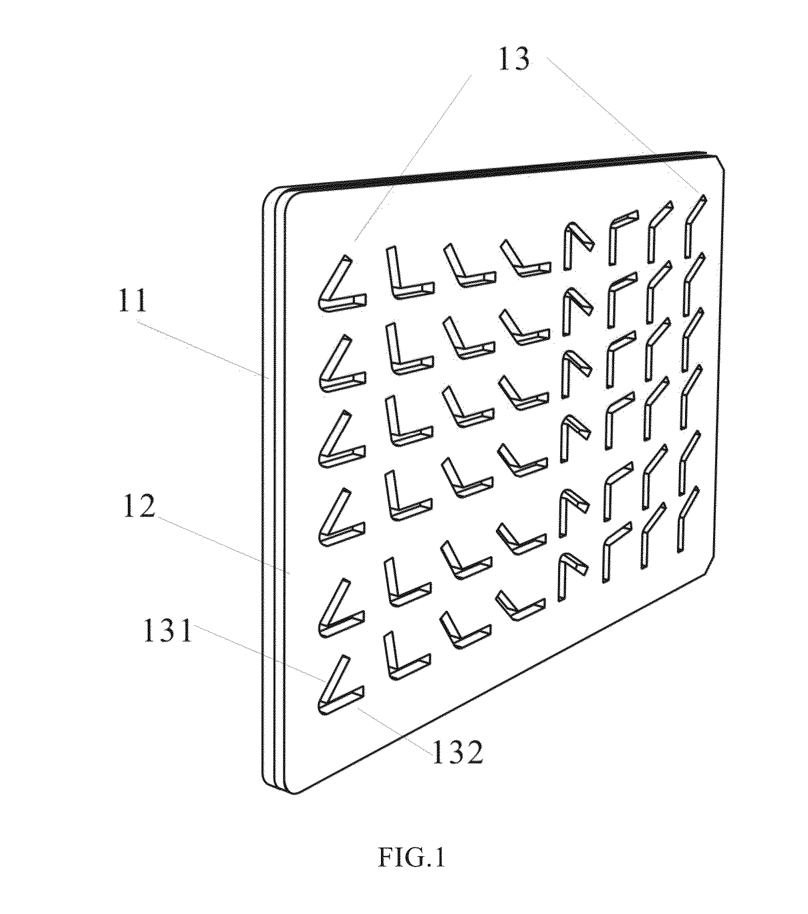
[0023]FIG. 1 is a diagram for showing the partial structure of the planar diffraction optical component which could be used to implement in full band beam shaping of spherical lens, spherical mirror, cylindrical lens, cylindrical mirror and other type of optical components.

[0024]As show in FIG. 1, the planar optical component comprises a substrate 11 and a metal film 12. The substrate 11 is made of a material having a high transmittance in optical wave band of interest, and has a thickness in the range of 300 μm˜1000 μm. The metal film 12 could use good conductor such as noble metal, for example gold, silver, copper and aluminum, with the thickness in the range of 100 nm˜1000 nm. The metal film 12 is set up on the substrate 11 and thus forming an interface with the substrate 11. A 2D thin antenna array 13 is set up on the metal film 12 and could be square array, circular array or other shapes array. The size of the thin array depends on the size of the incident light spot. The 2D th...

embodiment 2

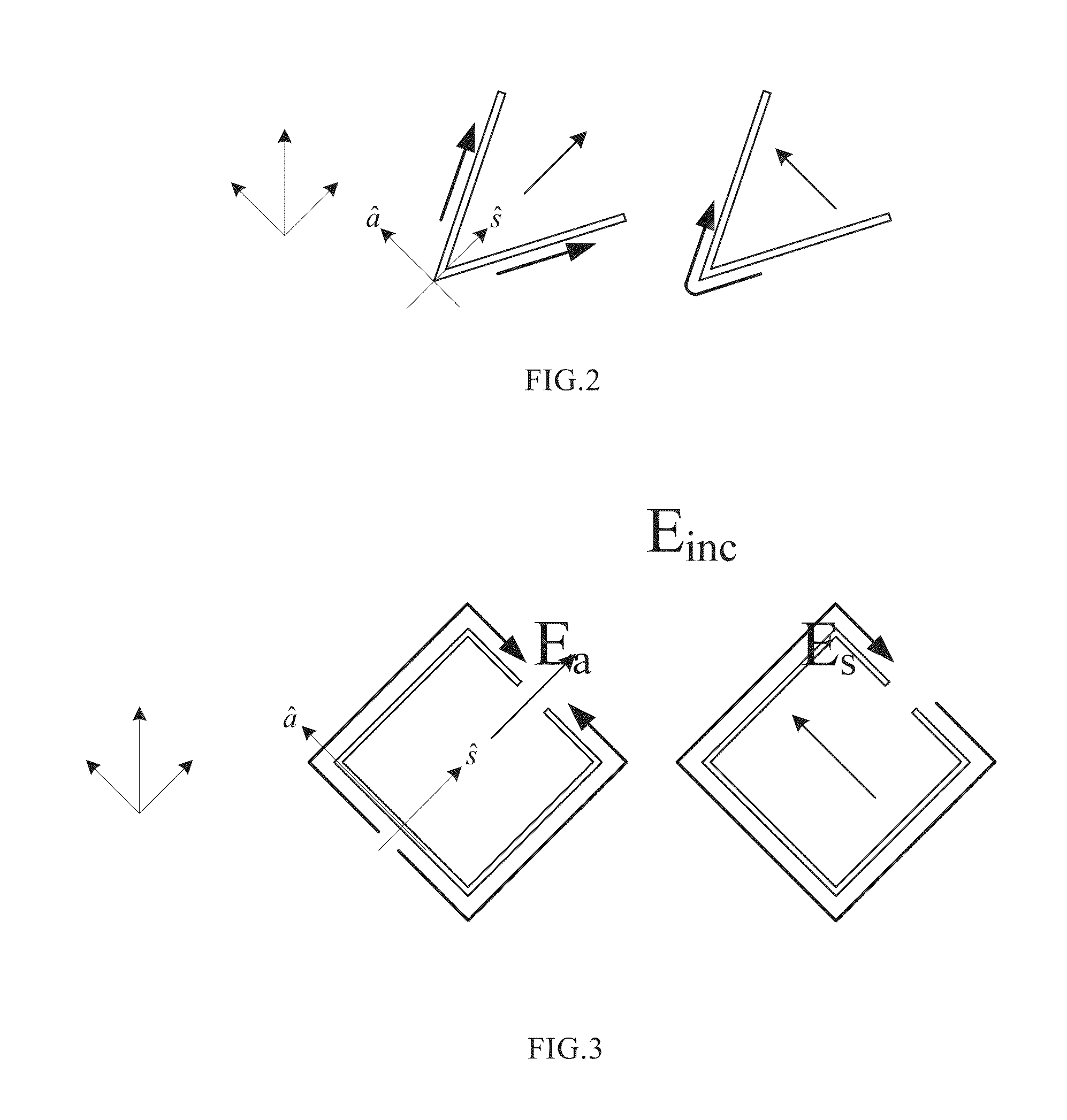
[0028]FIG. 3 shows electrical field excited by an antenna array element of rectangular structure having an opening according to another embodiment of the present invention. The embodiment of the invention defines two unit vectors, vector â and vector ŝ, to describe directions of the V-shaped antenna, the direction of vector ŝ being along symmetry axis of the antenna and the direction of vector â being perpendicular to the symmetry axis of the antenna, i.e., perpendicular to vector ŝ. As shown in FIG. 3, when the polarized light is incident on the antenna array element at a certain angle, the radiation field having electric fields of two mode, one being symmetric mode and the other being anti-symmetric mode, may be excited. In the electric field of symmetric mode, the current flows from the bottom of the rectangular antenna along both sides to the opening in the direction shown by the arrow; assuming that the rectangular antenna has a perimeter of 2h, the current distribution on each...


PUM


Abstract

This invention relates to a planar optical component and a design method thereof, the method including designing a structure with defined discrete phases; based on the structure with defined discrete phases as array elements, designing a 2D thin antenna array; constituting the planar optical component by a metal film having the 2D thin antenna array and a substrate. To achieve expected beam shaping effect, the method according to the embodiment of the present invention modulates structural parameters of antenna array elements to modulate the amplitude and phase of radiation field having vertical polarization states, which is excited by a beam having specific wavelengths and polarization states incident on the planar diffractive optical component. The planar diffractive optical component according to the embodiment of the present invention has little difference from expected parameters, and can achieve optimum beam shaping effect to make up the shortfall of conventional beam shaping elements.

Description

TECHNICAL FIELD[0001]The present invention relates to the field of optics, and more specifically to a planar optical component and its design method.BACKGROUND[0002]Traditional optical devices rely on gradual phase shifts accumulated during light propagation to achieve beam shaping. New degree of freedom in beam shaping could be obtained by introducing abrupt phase changes over the scale of the wavelength. An abrupt phase shift can be achieved by suitably engineering the interface between two different media. The phase discontinuity in the process of light propagation can be studied when the beam propagates across the interface of an optical resonator array having spacially varying phase response and sub wavelength interval. Equal amplitude conditions for the beam spreading along the interface and thus a constant phase gradient can be obtained by suitably designing the optical resonator. In the optical resonator, the phase shifts between outgoing light and the incident light may cha...

Claims


Application Information

Patent Timeline
IPC IPC(8): G02F1/01G06F17/50
CPCG06F17/50G02F1/01G02B5/3083H01Q15/0013H01Q15/006G02F2203/18G06F30/00
Inventor ZHANG, YANHU, DAN
Owner CAPITAL NORMAL UNIVERSITY
Why Eureka
Try Eureka