
Photocurable polymeric dielectrics and methods of preparation and use thereof

a polymer dielectric and polymer technology, applied in the field of photocurable polymer dielectrics and methods of preparation and use thereof, can solve the problems of inefficient curing of the dielectric film, short-wavelength uv rays and prolonged exposure, and need for high-energy light such as short-wavelength uv rays

Active Publication Date: 2014-12-11
FLEXTERRA INC
View PDF4 Cites 1 Cited by
  • Summary
  • Abstract
  • Description
  • Claims
  • Application Information

AI Technical Summary

Benefits of technology

[0002]Development of the next generation of electronic devices is based on organic materials, flexible substrates and low-cost solution-processing. A critical component in most organic electronic devices is a polymeric dielectric layer that serves as the gate insulator material in thin-film transistors, which are key building blocks of any electronic circuit. The polymer dielectric layer can be formed on either the gate contact (for bottom-gate transistor structures) or the semiconductor layer (for top-gate transistor structures) by depositing a solution of an electrically insulating (i.e., dielectric) polymer via a solution phase process such as spin-coating or printing. To create a robust, insoluble dielectric material, a crosslinking step usually is required.
[0003]Crosslinked dielectric films can be prepared by irradiation (i.e., photocuring), chemical initiators, or thermal treatment (i.e., annealing). Photocuring is advantageous because it can be easily implemented and can avoid chemical initiators or prolonged heating either of which can disrupt film uniformity. A limitation of several current-generation photocurable materials is the need for high-energy light such as short-wavelength UV rays and prolonged exposure to achieve sufficient curing. However, because many polymeric backbones and crosslinked units can absorb short-wavelength UV light, the use of these photocurable materials can lead to inefficient curing of the dielectric film. Therefore, it is advantageous to develop polymeric dielectric materials that can be crosslinked at longer wavelengths, which will lead to a faster and deeper cure of the dielectric layer.
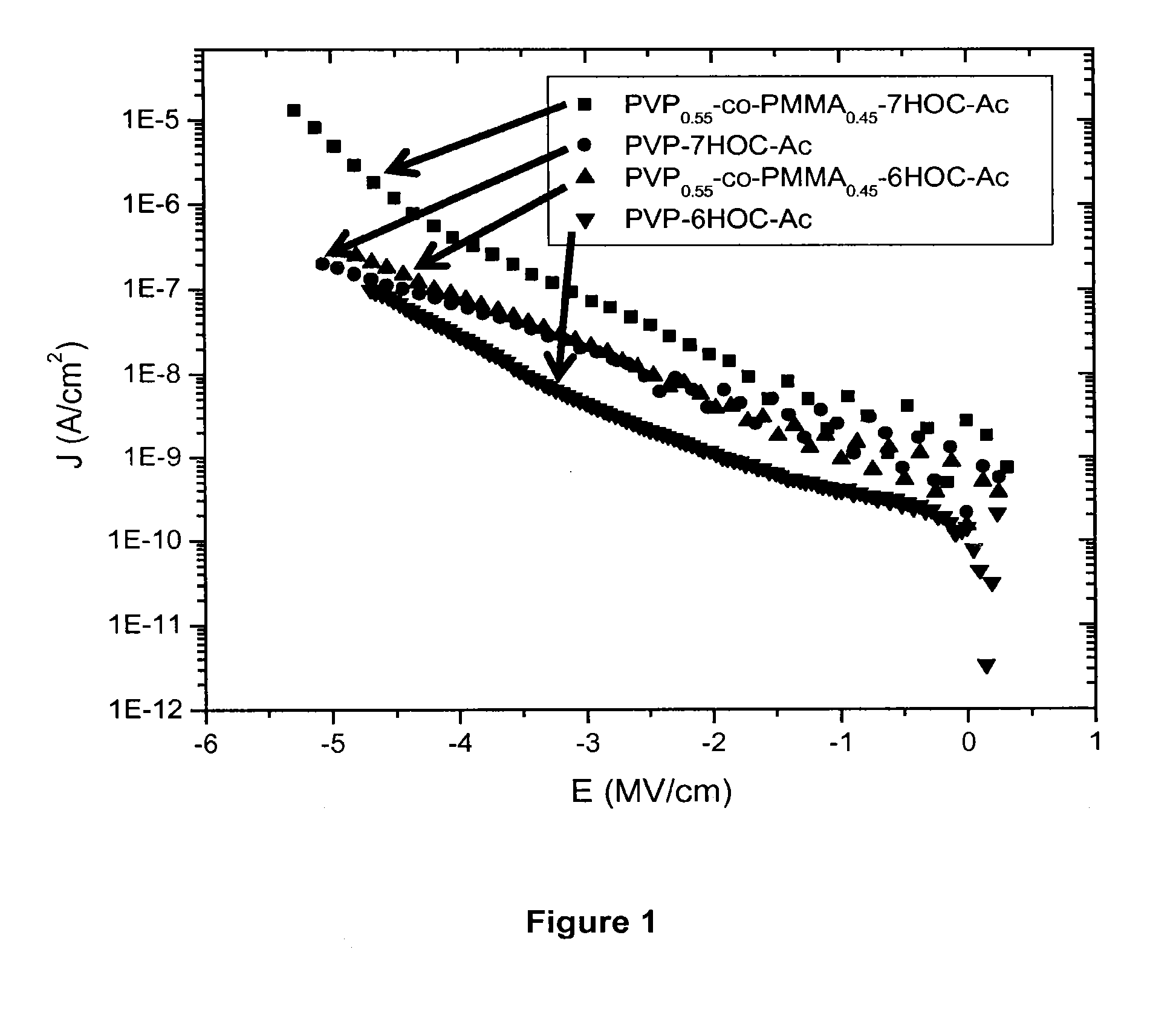
[0006]In one aspect, the present teachings provide various polymers and compositions including those polymers that can be used to prepare dielectric materials. Among other desirable properties, the polymers of the present teachings can be soluble in common organic solvents but can become insoluble in the same solvents after undergoing crosslinking, for example, photocrosslinking, which gives rise to certain processing advantages. More specifically, the present teachings provide polymers having crosslinkable functional groups, for example, photocrosslinkable functional groups, in their pendant groups (or side groups), enabling the polymers to crosslink, for example, upon radiation exposure. The crosslinking functionality can allow formation of a densely crosslinked polymeric matrix. Photopolymers of the present teachings and their crosslinked products can have excellent electrically insulating properties, which can enable their use as dielectrics. In some embodiments, the photopolymers and their crosslinked products can have a leakage current density that is less than or equal to about 1×10⁻⁸ A / cm2 at an electric field of 2 MV / cm.

Problems solved by technology

A limitation of several current-generation photocurable materials is the need for high-energy light such as short-wavelength UV rays and prolonged exposure to achieve sufficient curing.
However, because many polymeric backbones and crosslinked units can absorb short-wavelength UV light, the use of these photocurable materials can lead to inefficient curing of the dielectric film.

Method used


Image

  • Photocurable polymeric dielectrics and methods of preparation and use thereof
  • Photocurable polymeric dielectrics and methods of preparation and use thereof
  • Photocurable polymeric dielectrics and methods of preparation and use thereof

Examples


example 1

Preparation of 6Hoc-AcCl

[0125]

[0126]To a suspension of 25 g (0.15 mol) of 6-hydroxycoumarin and 30.7 g (0.22 mol) of K2CO3 in 550 mL of acetone was added 20.5 mL (30.9 g, 0.19 mol) of ethyl bromoacetate. The mixture was refluxed for 16 hours then filtered warm. The filtrate was concentrated in vacuo and the resulting solid was recrystallized from 100 mL of ethanol to give 34.8 g (91% yield) of 6Hoc-AcOEt as yellow prisms.

[0127]M.P. 113-114° C.; 1H NMR (500 MHz, CDCl3): δ 7.65 (d, 1H, J=8.5), 7.29 (d, 1H, J=9.5), 7.17 (d, 1H, J=8.7), 6.95 (s, 1H), 6.45 (d, 1H, J=9.8), 4.67 (s, 2H), 4.30 (q, 2H, J=6.5), 1.32 (t, 3H, J=6.8).

[0128]A mixture of 97 g (0.39 mol) of 6Hoc-AcOEt, 62 g (1.5 mol) of NaOH, 1 L of 1,4-dioxane, and 1.5 L of water was stirred at ambient temperature for 22 hours. The solution was treated with 150 mL of concentrated aqueous hydrochloric acid in one portion, with rapid stirring. The resulting suspension was cooled to room temperature and filtered. The filter cake was ...

example 2

Preparation of PVP0.55-co-PMMA0.45-6Hoc-Ac

[0132]

[0133]To a solution of 3.1 g of PVP-co-PMMA (MW 10 k, vinylphenol moiety molar ratio 55% based on calculation from proton NMR) and 10 mg of 4-dimethylamino-pyridine in 20 mL of pyridine was added a solution of 6.0 g (25 mmol) of 6Hoc-AcCl in 60 mL of hot 1,4-dioxane. The resulting mixture was stirred at ambient temperature for 3 hours then treated with 150 mL of methanol. The cloudy supernatant was decanted and the remaining residue was precipitated three times from 20 mL chloroform / 50 mL methanol, each time decanting the supernatant. The remaining residue was dissolved in 30 mL of chloroform and filtered directly into 100 mL of methanol cooled to −78° C. The precipitate was filtered off and dried in vacuo to give 6.3 g of PVP0.55-co-PMMA0.45-6Hoc-Ac as a white powder.

[0134]1H NMR (500 MHz, CDCl3):δ 7.67 (br s, 1H), 7.35-6.65 (m, 7H), 6.45 (br s, 1H), 4.9 (m, 2H), 3.5-0.5 (br).

example 3

Preparation of PVP0.80-co-PMMA0.20-6Hoc-Ac

[0135]

[0136]To a solution of 3.0 g of PVP0.80-co-PMMA0.20 (MW 70 k) and 10 mg of 4-dimethylaminopyridine in 15 mL of pyridine was added a solution of 7.5 g (31 mmol) of 6Hoc-AcCl in 75 mL of hot 1,4-dioxane. The resulting mixture was stirred at ambient temperature for 3 hours then treated with 100 mL of methanol. The supernatant was decanted and the remaining residue was treated with 30 mL of chloroform and stirred for 15 minutes. The mixture was treated with 100 mL of methanol and the supernatant was decanted. The remaining residue was precipitated three times from 20 mL cyclopentanone / 60 mL methanol, each time decanting the supernatant (traces of methanol were removed with a rotovap to aid dissolution in cyclopentanone). The remaining residue was dissolved in 60 mL of cyclopentanone and filtered directly into 300 mL of diethyl ether with rapid stirring. The precipitate was filtered off and washed with 3×50 mL of diethyl ether. The filter c...


PUM

PropertyMeasurementUnit
Tgaaaaaaaaaa
Tgaaaaaaaaaa
solubilityaaaaaaaaaa

Abstract

Disclosed are polymer-based dielectric compositions (e.g., formulations) and materials (e.g. films) and associated devices. The polymers generally include photocrosslinkable pendant groups; for example, the polymers can include one or more coumarin-containing pendant groups.

Description

CROSS REFERENCE TO RELATED APPLICATION[0001]This application claims priority to and the benefit of U.S. Provisional Patent Application Ser. No. 61 / 117,404, filed on Nov. 24, 2008, the disclosure of which is incorporated by reference herein in its entirety.INTRODUCTION[0002]Development of the next generation of electronic devices is based on organic materials, flexible substrates and low-cost solution-processing. A critical component in most organic electronic devices is a polymeric dielectric layer that serves as the gate insulator material in thin-film transistors, which are key building blocks of any electronic circuit. The polymer dielectric layer can be formed on either the gate contact (for bottom-gate transistor structures) or the semiconductor layer (for top-gate transistor structures) by depositing a solution of an electrically insulating (i.e., dielectric) polymer via a solution phase process such as spin-coating or printing. To create a robust, insoluble dielectric materia...

Claims


Application Information

Patent Timeline
Patent Type & Authority Applications(United States)
IPC IPC(8): H01B3/44C08F118/12B05D3/06C08F216/10
CPCH01B3/442C08F216/10B05D3/06H01B3/447C08F118/12H10K85/141H10K85/151H10K85/6574H10K10/471C09D125/18Y10T428/31938C08F212/22C08F212/32C08F220/14H10K10/00C08F12/24C08F12/22C08G61/02
Inventor QUINN, JORDANYAN, HEZHENG, YANNEWMAN, CHRISTOPHERKOEHLER, SILKE ANNIKAFACCHETTI, ANTONIOBREINER, THOMAS
Owner FLEXTERRA INC
Learn More