Oxide semiconductor TFT array substrate and method for forming the same

a technology of tft array substrate and oxidized semiconductor, which is applied in the direction of basic electric elements, semiconductor devices, electrical equipment, etc., can solve the problems of poor light stability, low migration rate, and complex structur

Active Publication Date: 2014-12-25
SHANGHAI TIANMA MICRO ELECTRONICS CO LTD +1
View PDF4 Cites 8 Cited by
  • Summary
  • Abstract
  • Description
  • Claims
  • Application Information

AI Technical Summary

Benefits of technology

[0010]One inventive aspect is an oxide semiconductor TFT array substrate. The substrate includes a thin film transistor having a gate, a first part of a gate insulation layer on the gate, and an active layer on the first part of the gate insulation layer, where the active layer includes an oxide semiconductor layer. The thin film transistor also has a first part of an etch barrier layer on the active layer, and a source and a drain on the first part of the etch barrier layer. The substrate also includes a storage capacitance having a first electrode plate, a second part of the gate insulation layer on the first electrode plate, a second part of the etch barrier layer on the second part of the gate insulation layer, and a second electrode plate on the second part of the etch barrier layer. In addition, at least one of: the second part of the etch barrier layer above the first electrode plate has a thickness less than a thickness of the first part of the etch barrier layer above the gate, and there is no etch barrier layer disposed between the second part of the gate insulation layer and the second electrode plate.

Problems solved by technology

However, current p-Si TFTs may only be used in products with medium or small sizes due to the limitation of film uniformity thereof Specifically, a-Si TFTs have advantages like simple structure and high uniformity for mass production, and drawbacks like low migration rate (about 0.5 cm2 / V·s) and poor light stability.
Although p-Si TFTs have a migration rate (normally larger than 10 cm2 / V·s) much larger than that of a-Si TFTs, they have disadvantages such as complex structure, large leakage current and poor uniformity for mass production.
However, conventional a-Si TFTs and p-Si TFTs may not be capable of meeting the requirements.
In conclusion, currently, increasing the capacitance value of the storage capacitance in the TFT array substrate may result in reducing the aperture opening rate or deteriorate the device performance.

Method used


Image

  • Oxide semiconductor TFT array substrate and method for forming the same
  • Oxide semiconductor TFT array substrate and method for forming the same
  • Oxide semiconductor TFT array substrate and method for forming the same

Examples


first embodiment

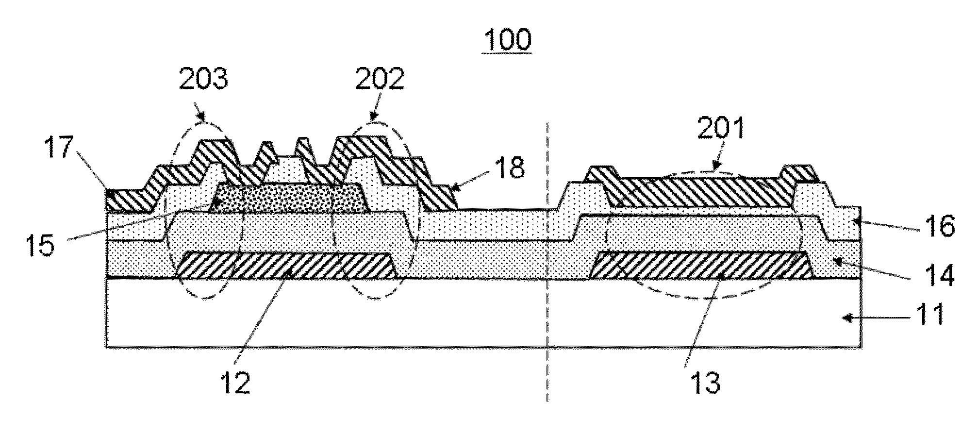
[0021]An oxide semiconductor TFT array substrate is provided according to a first embodiment of the present disclosure. FIG. 2 schematically illustrates a cross-sectional view of an oxide semiconductor TFT array substrate 100 according to a first example of the first embodiment of the present disclosure. Referring to FIG. 2, the oxide semiconductor TFT array substrate 100 includes a substrate 11, and a thin film transistor and a storage capacitance 201 on the substrate 11.

[0022]The thin film transistor includes a gate 12, a first part of a gate insulation layer 14 on the gate 12, an active layer 15 on the first part of the gate insulation layer 14, a first part of an etch barrier layer 16 on the active layer 15, and a source 17 and a drain 18 on the first part of the etch barrier layer 16. The active layer 15 is an oxide semiconductor layer. Specifically, the active layer 15 may include indium-gallium-zinc-oxide (IGZO).The source 17 and the drain 18 are respectively coupled to the a...

second embodiment

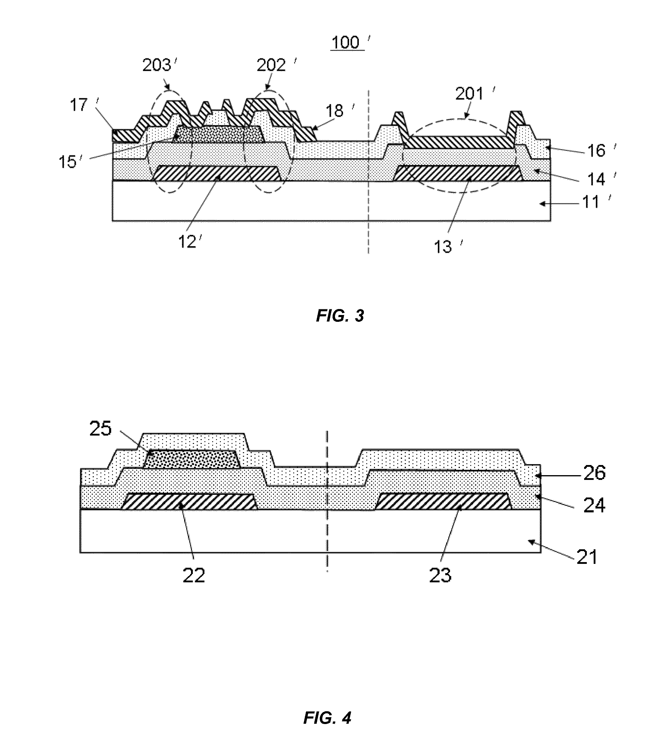
[0032]According to a second embodiment of the present disclosure, a method for forming an oxide semiconductor TFT array substrate is provided. FIGS. 4 to 6 schematically illustrate cross-sectional views of intermediate structures formed in a process forming an oxide semiconductor TFT array substrate according to a first example of the second embodiment.

[0033]Referring to FIG. 4, in step 1, a substrate 21 is provided. The substrate 21 may be a glass substrate or a flexible substrate.

[0034]Thereafter, in step 2, a first conducting layer is formed on the substrate 21. The first conducting layer may be a metal layer.

[0035]Thereafter, in step 3, the first conducting layer is etched with a first mask to form a gate 22 of a thin film transistor and a first electrode plate 23 of a storage capacitance. The first electrode plate 23 of the storage capacitance may be disposed inside a pixel region or in a circuit in peripheral areas of the pixel region.

[0036]In step 4, a gate insulation layer 2...

third embodiment

[0046]According to a third embodiment of the present disclosure, a method for forming an oxide semiconductor TFT array substrate is provided. Processing steps 1 to 7 of the method provided by the third embodiment are the same as those in the second embodiment, which may not be illustrated in detail here.

[0047]A difference lies in step 8, compared with the second embodiment. Specifically, referring to FIG. 8, after a first part of an etch barrier layer 36 above a first electrode plate 33 is etched out, the etch process continues to etch a corresponding part of a gate insulation layer 34 under the first part of the etch barrier layer until the corresponding part of the gate insulation layer 34 is partially removed to obtain a desired thickness.

[0048]Thereafter, in step 9, a second conducting layer is formed on the reminded etch barrier layer 36. Portions of the second conducting layer are deposited into through holes of the reminded etch barrier layer 36. In step 10, the second conduc...


PUM


Abstract

A TFT array substrate is disclosed. The substrate includes a TFT having a gate insulation layer, and an active layer partly thereon. The TFT also has a first part of an etch barrier layer on the active layer, and a source and drain on the first part of the etch barrier layer. The substrate also includes a capacitance having a first electrode plate, a second part of the gate insulation layer on the first electrode plate, a second part of the etch barrier layer on the second part of the gate insulation layer, and a second electrode plate on the second part of the etch barrier layer. The second part of the etch barrier layer has a thickness less than the first part of the etch barrier layer, and/or there is no etch barrier layer between the second part of the gate insulation layer and the second electrode plate.

Description

CROSS-REFERENCES TO RELATED APPLICATIONS[0001]The present application claims the benefit of priority to Chinese Patent Application No. 201310254826.6, entitled “OXIDE SEMICONDUCTOR TFT ARRAY SUBSTRATE AND METHOD FOR FORMING THE SAME”, filed with the Chinese Patent Office on Jun. 24, 2013, the content of which is incorporated herein by reference in its entirety.FIELD OF THE DISCLOSURE[0002]The present disclosure generally relates to semiconductor technology, and more particularly, to an oxide semiconductor TFT array substrate and a method for forming the same.BACKGROUND OF THE INVENTION[0003]Currently, thin-film-transistor (TFT) technology is widely used in the technical field of panel displays including liquid crystal displays, organic emitting displays, and the like. Conventionally, active layers used in TFT technology may normally include a semiconductor material such as amorphous silicon (a-Si), polycrystalline silicon (p-Si), or the like. Among the conventional TFTs, a-Si TFTs a...

Claims


Application Information

Patent Timeline
Patent Type & Authority Applications(United States)
IPC IPC(8): H01L27/12
CPCH01L27/127H01L27/1225H01L27/1255
Inventor LOU, JUNHUIHOU, SITAO
Owner SHANGHAI TIANMA MICRO ELECTRONICS CO LTD
Why Eureka
Try Eureka