Charge-sensitive amplifier

a technology of amplifiers and charge-sensitive pads, which is applied in the direction of amplifiers, amplifiers with field-effect devices, analog and hybrid computing, etc., can solve the problems of reducing fet gain, difficult to work with bond pads with diameters smaller than 70 micrometres, and difficult to position wire bonds within the boundary of pads. , to achieve the effect of optimizing manufacturing productivity

Active Publication Date: 2015-01-29
OXFORD INSTR NANOTECH TOOLS
View PDF6 Cites 7 Cited by
  • Summary
  • Abstract
  • Description
  • Claims
  • Application Information

AI Technical Summary

Benefits of technology

[0019]In most cases the charge-sensitive amplifier comprises a substrate positioned beneath the region of relatively low doping, the substrate being formed from a highly doped extrinsic semiconductor material of a second type, different from the first. This may be electrically biased when in use to ensure electrical isolation at the “pn” junction region between the first and second types. An electrical connection to such a substrate may also be provided using a pad deposited upon the surface of the field effect transistor. The effect of the relative position of the highly doped capacitor plate therefore provides electromagnetic shielding of the gate pad from the substrate. Thus the relative arrangement of the gate pad and capacitor causes a capacitance between the gate pad and the “ground” to be substantially less than the total capacitance experienced at the gate.
[0020]The charge-sensitive amplifier may be arranged in two possible alternative configurations. It may be firstly connected to the field effect transistor in a “source follower” configuration in which the amplifier is connected to the source. It may alternatively be connected in a “common source configuration” in which the amplifier is connected to the drain of the field effect transistor.
[0021]The invention is not intended to be limited to any specific type of field effect transistor and therefore it may be implemented with each of JFET or MOSFET devices. Thus it will be appreciated, the present invention finds particular application in arrange

Problems solved by technology

Discrete FETs can in principle be made with much smaller input capacitance than 1 pF but when the FET input capacitance is reduced by shrinking the dimensions of the FET, this also reduces the FET gain.
If a pad is made smaller it makes it harder to position the wire bond within the boundary of the pad.
With commonly-available bonding equipment, it is difficult to work with bond pads that have diameter smaller than 70 micrometres.
However, when this approach is used, it is di

Method used


Image

  • Charge-sensitive amplifier
  • Charge-sensitive amplifier
  • Charge-sensitive amplifier

Examples


Embodiment Construction

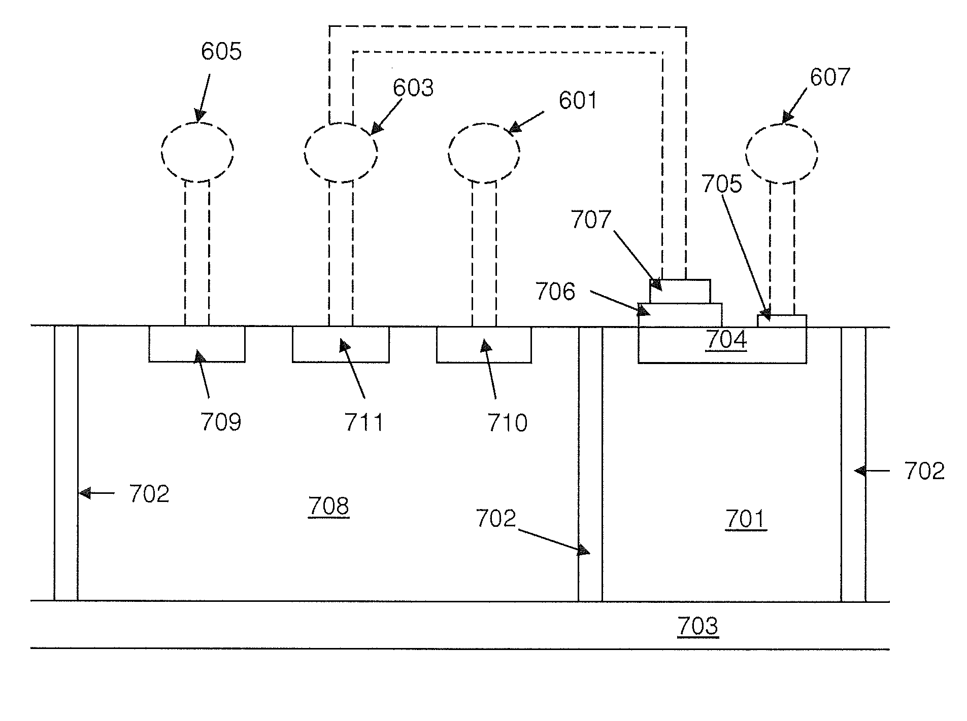
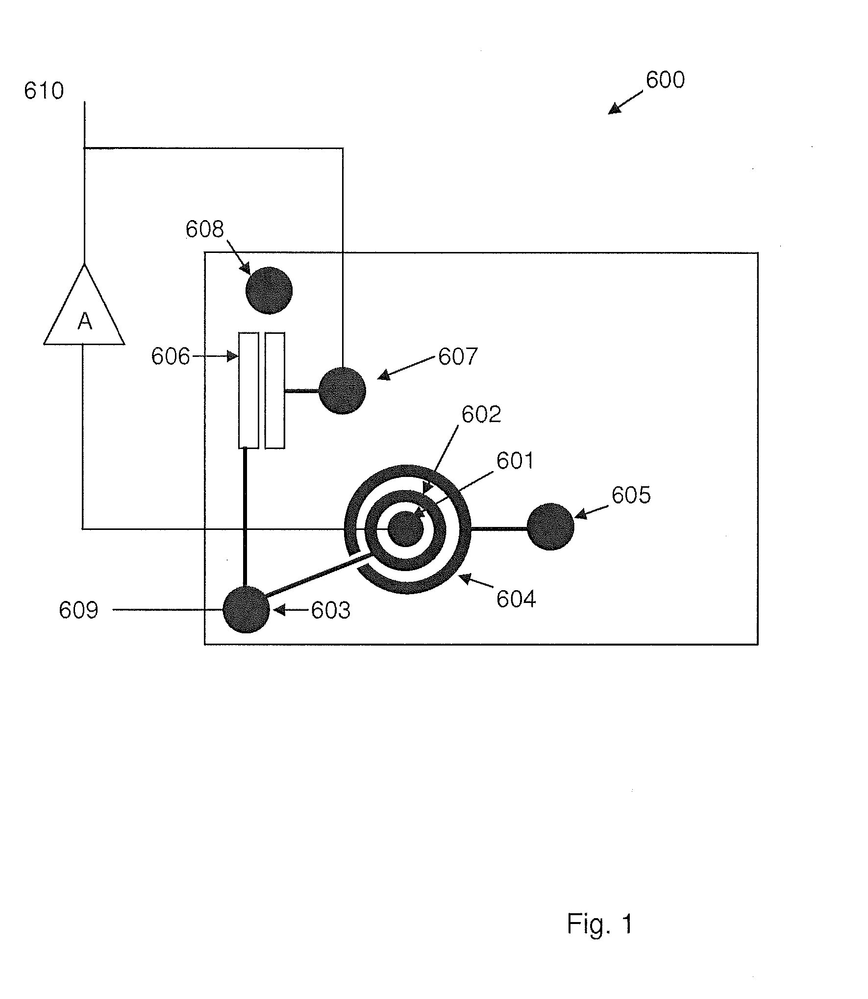
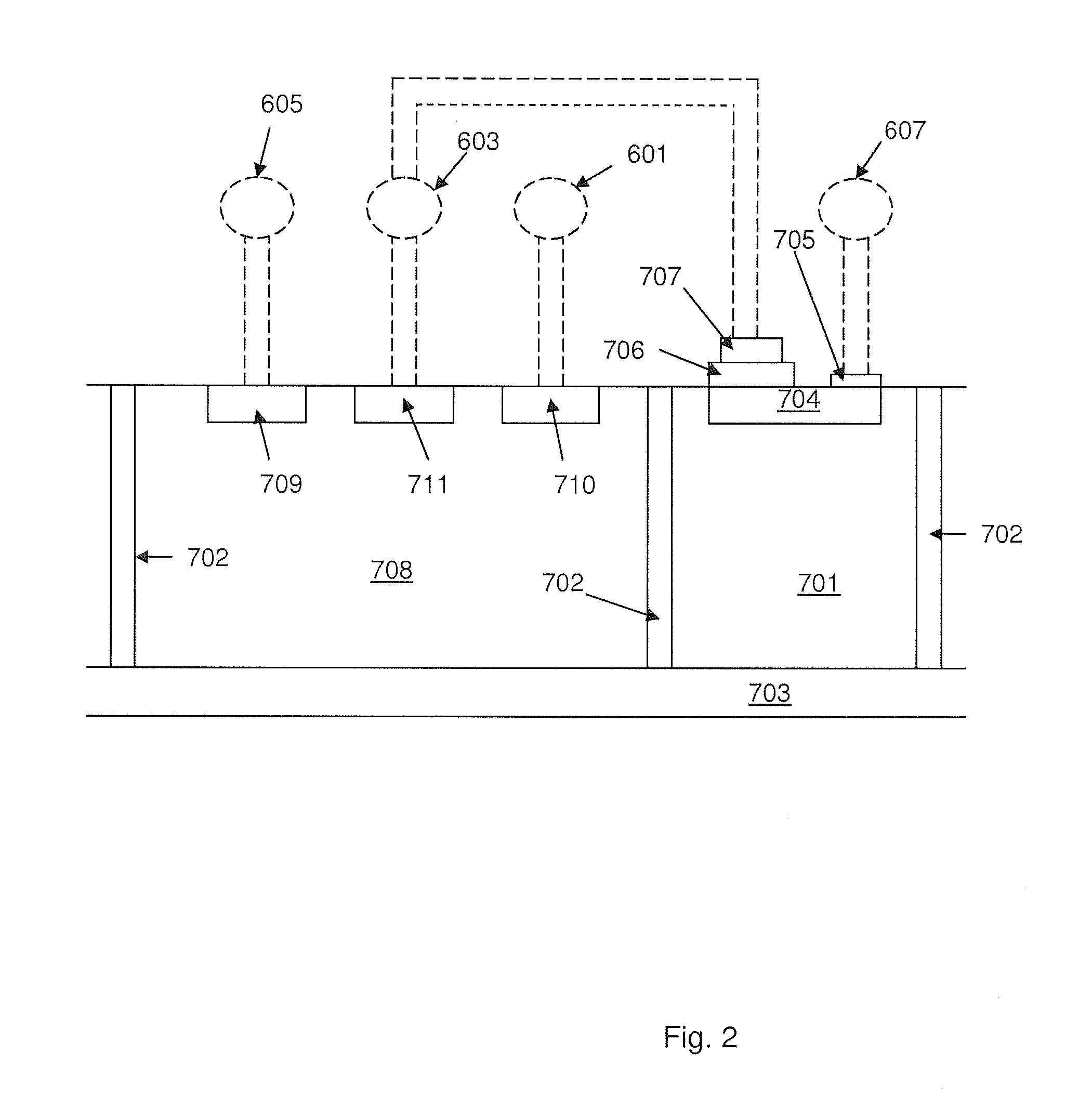
[0029]The invention exploits a feature which is commonly used in radiation detection systems to achieve a “charge sensitive amplifier” (CSA). The output voltage step from a CSA is proportional to the increment of charge deposited at the input and is independent of the capacitance of the detector connected to the input. Since the increment of charge released by the detector is proportional to the energy of the incident radiation particle, the output voltage step from a CSA is also proportional to the energy of the particle. An example of such a CSA is described in GB 2305776. With reference to FIG. 5 of GB 2305776, the key components of a CSA are the high gain amplifier A and a feedback capacitor 512 that connects the low impedance output of the amplifier to the high impedance sensitive gate, G, of the FET that is also connected to the detector by connection 502.

[0030]The FET device is typically a small die with dimension approximately 1 mm by 1 mm and connections to the electrodes o...


PUM


Abstract

A charge-sensitive amplifier is disclosed for use in amplifying signals from a particle detector. This includes a field effect transistor having a gate, source and drain, the gate being connectable, using a gate pad, to the particle detector, for the receipt of said signals. Also included is an amplifier having an input connected to the drain or source of the field effect transistor and an output connected through a feedback capacitor to the gate of the field effect transistor. The gate pad of the field effect transistor is made to be integral with the feedback capacitor so as to reduce the capacitance of the device.

Description

FIELD OF THE INVENTION[0001]The present invention relates to the field of radiation detection and imaging. In particular, the present invention relates to an apparatus for improving the performance of semiconductor radiation detectors for detection and measurement of energetic particles, such as x-ray photons. The inventive apparatus is in the form of a charge-sensitive amplifier for use in amplifying signals from a particle detector. The present invention finds particular advantage in x-ray detection systems where a Field Effect Transistor (FET) is bonded to a semiconductor detector element and used in a “charge-sensitive” amplifier configuration. The invention provides a method to reduce the overall capacitance and thus improve the resolution of the detector as a whole.BACKGROUND TO THE INVENTION[0002]For the last 40 years there has been ongoing development of semiconductor radiation detectors to achieve increased sensitivity, higher energy resolution, lower electronic noise and l...

Claims


Application Information

Patent Timeline
IPC IPC(8): H03F3/16G01T1/17
CPCG01T1/17H03F3/16H01L29/41758H01L29/808H01L29/94H03F3/082H03F3/70H01L27/0629G06G7/186
Inventor NASHASHIBI, TAWFIC
Owner OXFORD INSTR NANOTECH TOOLS
Why Eureka
Try Eureka