Method for Modifying Properties of Graphene

a graphene and property technology, applied in the field of graphene property modification, can solve the problems of inapplicability of the above methods, easy damage to the semiconductor film, and serious damage, so as to avoid damage to the graphene material, effectively control the bonding effect, and alter the energy band characteristics of the graphene film

Inactive Publication Date: 2015-04-30
METAL INDS RES & DEV CENT
View PDF1 Cites 2 Cited by
  • Summary
  • Abstract
  • Description
  • Claims
  • Application Information

AI Technical Summary

Benefits of technology

[0017]In the method for modifying properties of graphene according to the present invention, the graphene film is radiated with an electron beam to effectively control the it bond of the graphene film, altering the energy band characteristics of the graphene film and obtaining the graphene material with semiconductor properties.
[0018]Furthermore, in the method for modifying properties of graphene according to the present invention, the graphene film is radiated with an electron beam in a low temperature environment to avoid damage to the graphene material resulting from a high temperature environment. The subsequent procedures for repairing damaged graphene material is, thus, not required, simplifying the producing procedures and reducing the industrial costs.
[0019]The method for modifying properties of graphene according to the present invention uses an electron beam that can be accurately located and can be qualitatively controlled. Thus, a small modification area can be scanned with the electron beam. Furthermore, the current intensity (e.g., 70-120 pA), the scanning time (e.g., 0.1-0.4 μms per point), and the accelerating voltage (e.g., 50 KeV) of the electron beam can respectively be controlled such that the radiating energy of the electron beams is in a range of 200-1200 μC / cm2, which is sufficient to modify the semiconductor properties to different extents (i.e., the property modification extent of graphene). Thus, different property modification needs of different products can be fulfilled, which is an effect of the present invention.

Problems solved by technology

However, thermal diffusion must be carried out in a high temperature environment that easily damages the semiconductor film.
Although ion implantation can be carried out without a high temperature environment, the collision between ionized elements causes serious damage to the structure of the semiconductor film and, thus, requires annealing to repair the structure.
Although the above methods can be used to modify the structural properties of semiconductor films, serious damages are caused due to the small thickness (about 0.34 nm) of graphene.
Namely, the above methods are not suitable.
Modification to properties of a small area graphene is difficult.

Method used


Image

  • Method for Modifying Properties of Graphene
  • Method for Modifying Properties of Graphene

Examples


Embodiment Construction

[0024]A method for modifying properties of graphene according to the present invention includes a graphene film provision step and a modification step to obtain a graphene material.

[0025]Specifically, the graphene film provision step includes providing a graphene film. The graphene film is formed on a substrate. The substrate can be a surface of an electric element or transistor, and graphene is formed on the surface. The substrate can be made of silicon, glass, or plastic.

[0026]Graphene can be formed on the substrate by any method, such as chemical vapor deposition, physical vapor deposition, or mechanical exfoliation, which is known in the art.

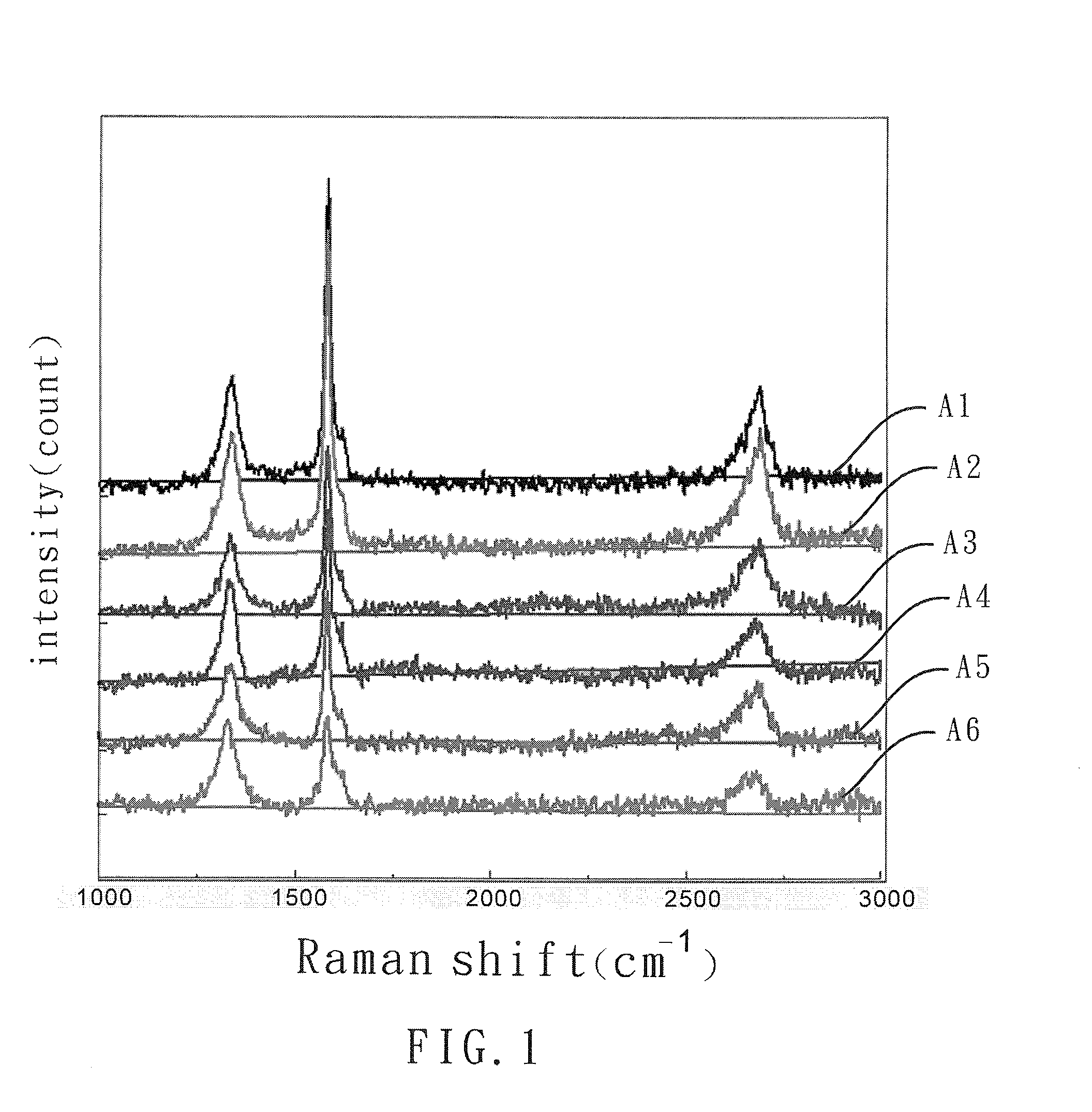
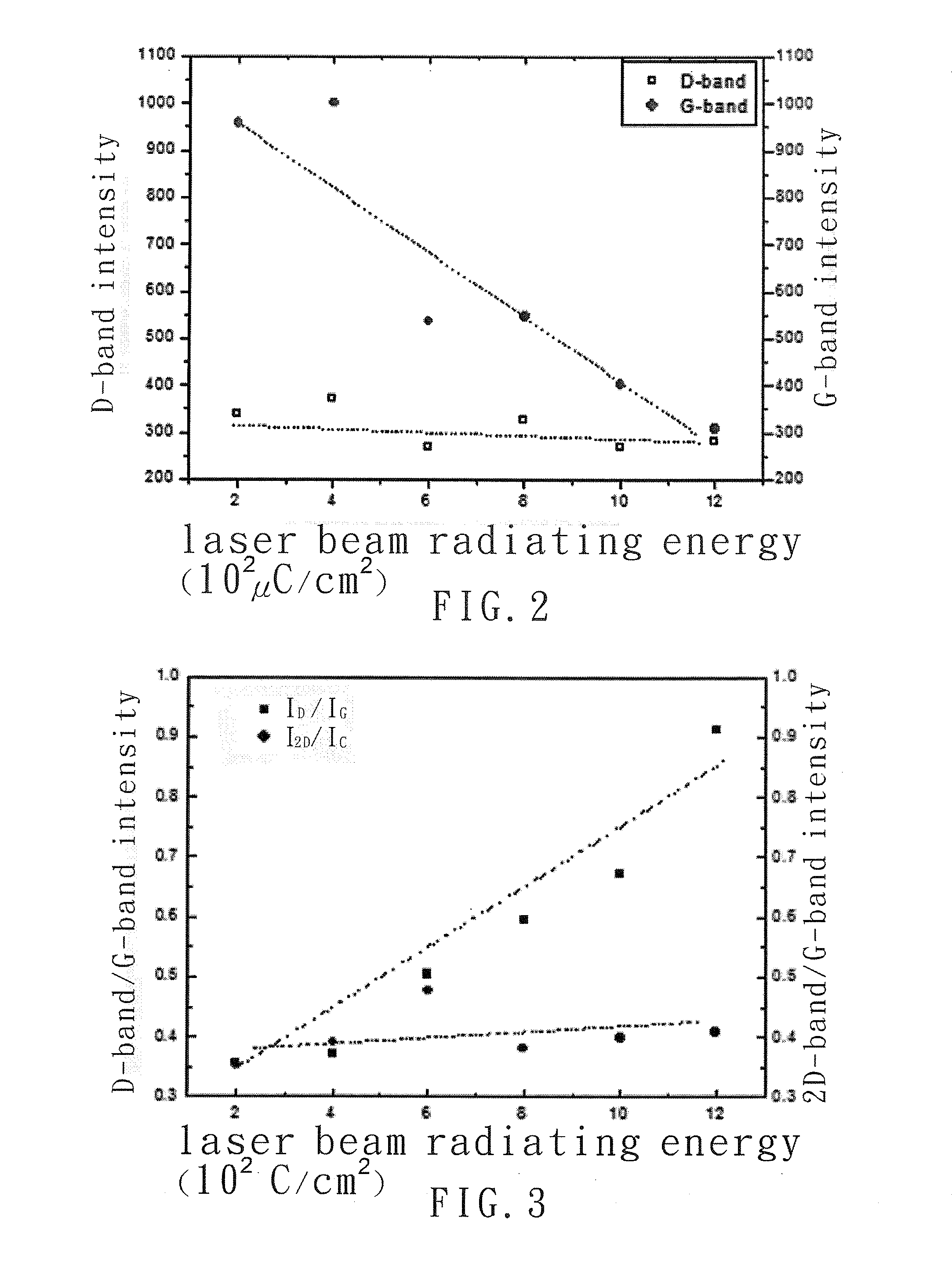
[0027]The graphene material is obtained after the modification step modifying properties of the graphene film. Specifically, the graphene film is placed in a vacuum environment and is radiated with an electron beam. In the preferred embodiment, the electron beam has an accelerating voltage of 50 KeV, has a radiating energy in a range of 200-...


PUM

PropertyMeasurementUnit
current intensityaaaaaaaaaa
thicknessaaaaaaaaaa
temperatureaaaaaaaaaa

Abstract

A method for modifying properties of graphene includes a graphene film provision step and a modification step. In the graphene film provision step, a graphene film is provided, and the graphene is formed on a substrate. In the modification step, the graphene film is placed in a vacuum environment and radiated by an electron beam to obtain a graphene material.

Description

BACKGROUND OF THE INVENTION[0001]1. Field of the Invention[0002]The present invention relates to a method for modifying properties of graphene and, more particularly, to a method for modifying semiconductor properties of graphene.[0003]2. Description of the Related Art[0004]Graphene is a substantially plan film having hexagonal lattices and is a two-dimensional material having a thickness (about 0.34 nm) of a carbon atom. In addition to excellent properties including high mechanical strength, high thermal conduction, and high carrier transfer efficiency, the semiconductor properties of graphene can be modified to develop electric elements or transistors that are thinner and that have a higher current conduction speed.[0005]Conventional methods for modifying semiconductor properties include thermal diffusion and ion implantation. In thermal diffusion, atoms to be doped are driven by a high temperature not lower than 500° C. into a semiconductor film and a substrate coupled to the sem...

Claims


Application Information

Patent Timeline
Patent Type & Authority Applications(United States)
IPC IPC(8): B01J19/08
CPCB01J19/085C01B32/194H01L21/02527H01L21/02664
Inventor HUANG, CHIA-HUNGCHU, CHI-WENCHIU, SUNG-MAOWANG, CHUN-CHIEHWEI, CHIA-MINCHUNG, CHUNG-JENWU, BO-HSIUNG
Owner METAL INDS RES & DEV CENT
Why Eureka
Try Eureka