Sensor using sensing mechanism having combined static charge and field effect transistor

a sensing mechanism and transistor technology, applied in the direction of instruments, device details, piezoelectric/electrostrictive device details, etc., can solve the problems of large change of sensitivity of the sensor, low sensitivity of the entire sensor, and inability to accurately convert the capacitance change into electrical output signals, etc., to achieve simplified configuration, small shape, and improve sensitivity

Inactive Publication Date: 2015-04-30
POSTECH ACAD IND FOUND
View PDF3 Cites 11 Cited by
  • Summary
  • Abstract
  • Description
  • Claims
  • Application Information

AI Technical Summary

Benefits of technology

[0028]The sensor using the sensing mechanism combining an electrostatic unit and an electric field effect transistor according to an exemplary embodiment of the present invention measures the change of the electric field of the channel part of the electric field effect transistor by using the electrostatic member to measure the displacement or the dynamic of the sensor such that the electric field that is proportional to the charge amount and is inversely proportional to the distance regardless of the intensity and the distribution of the external electric field may be formed, thereby improving the sensitivity without the influence of the external electric field.
[0029]Further, the conventional sensor using the electrode needs the additional ground electrode to form the electric field, however the sensor using the sensing mechanism combining the electrostatic unit and the electric field effect transistor according to the exemplary embodiment of the present invention does not need the additional ground electrode to form the electric field such that the configuration is simplified.
[0030]Also, by using the electric field effect transistor, electrical impedance of a low degree may be maintained in a very small shape such that sensitivity of a low frequency may be obtained.
[0031]In addition, the sensor may be sufficiently realized through only the interface circuit of the simple structure by the low electrical impedance and the separate circuit is not needed for the active biasing by using the semi-permanent electrostatic member (the electret) or piezoelectric member, thereby reducing additional power consumption.
[0032]Also, the sensor using the sensing mechanism combining the electrostatic unit and the electric field effect transistor according to the exemplary embodiment of the present invention as the method in which the electric field generated by the electrostatic member (the electret) or the bound charge of the piezoelectric member is applied to the electric field effect transistor forms the strong electric field by using the electrostatic unit and the bound charge compared with the conventional sensor using the electric field effect transistor using the electrode, thereby obtaining high sensitivity.

Problems solved by technology

To change the electrical state change of the electric element into the electric output, a current is needed such that the correct conversion of the capacitance change into the electrical output signal has a limitation.
However, due to the low mechanical-electrical conversion efficiency of the piezoresistive material, there is a drawback that the entire sensitivity is relatively low compared with other methods, and a change of the sensitivity of the sensor is largely generated according to temperature.
In the case of the piezoelectric type of sensor, since the output signal having a relatively large size may be obtained without the addition of the bias voltage, it has been largely applied to a sound sensor such as the microphone or a hydrophone until now, however it is the reversible conversion method such that it may be not free from the unique characteristic.
Accordingly, since the size of the piezoelectric member used is minutely small if extreme down-sizing is realized, the charge amount that may be generated by the pressure is extremely small such that the conventional circuital measuring method may not satisfy the required sensitivity, the frequency band, and a noise for the signal.
Particularly, an increase of electric impedance according to the down-sizing causes deterioration of the low frequency performance.
The capacitive type of sensor is widely applied to a very small pressure sensor, sound sensor, and acceleration-based sensor, however it is the reversible energy conversion like the piezoelectric sensor such that the capacitance of the sensor is extremely small according to the extreme down-sizing, and the sensitivity deterioration effect due to parasitic capacitance appears.
However, although the sensor and the interface circuit are integrated and the sensitivity is preserved, the capacitive type of sensor may not avoid the deterioration of the sensitivity of the low frequency region and the noise characteristic according to the extreme down-sizing.
It is difficult to solve the problem of the low frequency characteristic and the sensitivity due the technical and electrical conversion method of the sensor through the high performance and the optimization of the interface circuit.
The piezoresistive type and this type use non-reversible energy conversion methods such that the limitation of the output signal is not determined by the dynamic of the sensor.
However, the optical type of sensor has drawbacks such as the change of sensitivity according to the sensor temperature and the difficult aligning and calibration of optics in spite of the several merits such as the sensitivity.
As described above, the capacitive type and the piezoelectric type adopted in the conventional sensor have the limitation such as the deterioration of the sensitivity and the low frequency performance according to the extreme down-sizing, and the optical type and the piezoresistive type do not have the deterioration of the frequency performance according to the down-sizing, but are different to be itself down-size or have the problem a noise ratio for a signal does not reach a required degree.

Method used


Image

  • Sensor using sensing mechanism having combined static charge and field effect transistor
  • Sensor using sensing mechanism having combined static charge and field effect transistor
  • Sensor using sensing mechanism having combined static charge and field effect transistor

Examples


Embodiment Construction

[0037]Hereinafter, the present invention will be described more fully hereinafter with reference to the accompanying drawings, in which exemplary embodiments of the invention are shown. As those skilled in the art would realize, the described embodiments may be modified in various different ways, all without departing from the spirit or scope of the present invention.

[0038]A part irrelevant to the description will be omitted to clearly describe the present invention, and the same elements will be designated by the same reference numerals throughout the specification.

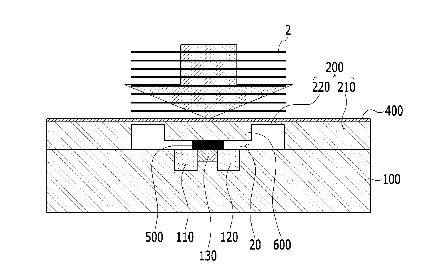
[0039]Now, a sensor using a sensing mechanism combining an electrostatic unit and an electric field effect transistor according to a first exemplary embodiment of the present invention will be described with reference to FIG. 1.

[0040]FIG. 1 is a cross-sectional view of a sensor using a sensing mechanism combining an electrostatic unit and an electric field effect transistor according to a first exemplary embodiment of th...


PUM


Abstract

The present invention relates to a sensor that uses a sensing mechanism having a combined static charge and a field effect transistor, the sensor including: a substrate; source and drain units formed on the substrate and separated from each other; a channel unit interposed between the source and drain units; a membrane separated from the channel unit, disposed on a top portion and displaced in response to an external signal; and a static charge member formed on a bottom surface of the membrane separately from the channel unit and generating an electric field. Accordingly, since the sensor using a sensing mechanism having a combined static charge and a field effect transistor according to an embodiment of the present invention can measure the displacement or movement of the sensor by measuring a change of the electric field of the channel unit of the field effect transistor by using a static member, the electric field can be formed so as to be proportional to an amount of charge and inversely proportional to a squared distance regardless of the intensity and distribution of an external electric field. Therefore, sensitivity is improved without being affected by an external electric field.

Description

TECHNICAL FIELD [0001]The present invention relates to a sensor using a mechanism sensing an energy conversion in which a change of mechanical and physical amounts is converted into an electrical signal by combining an electrostatic unit and an electric field effect transistor.BACKGROUND ART [0002]Most devices include an element converting energy. Particularly, in a case of a sensor, an electrical output is mostly required such that at least one energy conversion is processed within the device. For example, in a case of a capacitive type of microphone that is widely used, displacement of a thin film that is deformed by a pressure wave of a sound changes a capacitance with an electrode positioned near the thin film, and the change of capacitance changes an electrical state that was formed in a balance state by a bias voltage that is initially applied, thereby generating a voltage change or a charge of change amount between the thin film and the electrode. If they are connected to an ...

Claims


Application Information

Patent Timeline
Patent Type & Authority Applications(United States)
IPC IPC(8): H01L29/84H01L41/04H01L41/113
CPCH01L29/84H01L41/04H01L41/1132B81B3/0021B81B2201/0257B81B2201/0264G01P15/08G01L9/0072G01L9/008H04R23/006H04R2201/003H10N30/80H10N30/302
Inventor MOON, WON KYUWEST, JAMES EDWARDSUNG, MINJE, YUBSHIN, KUM JAE
Owner POSTECH ACAD IND FOUND
Why Eureka
Try Eureka