

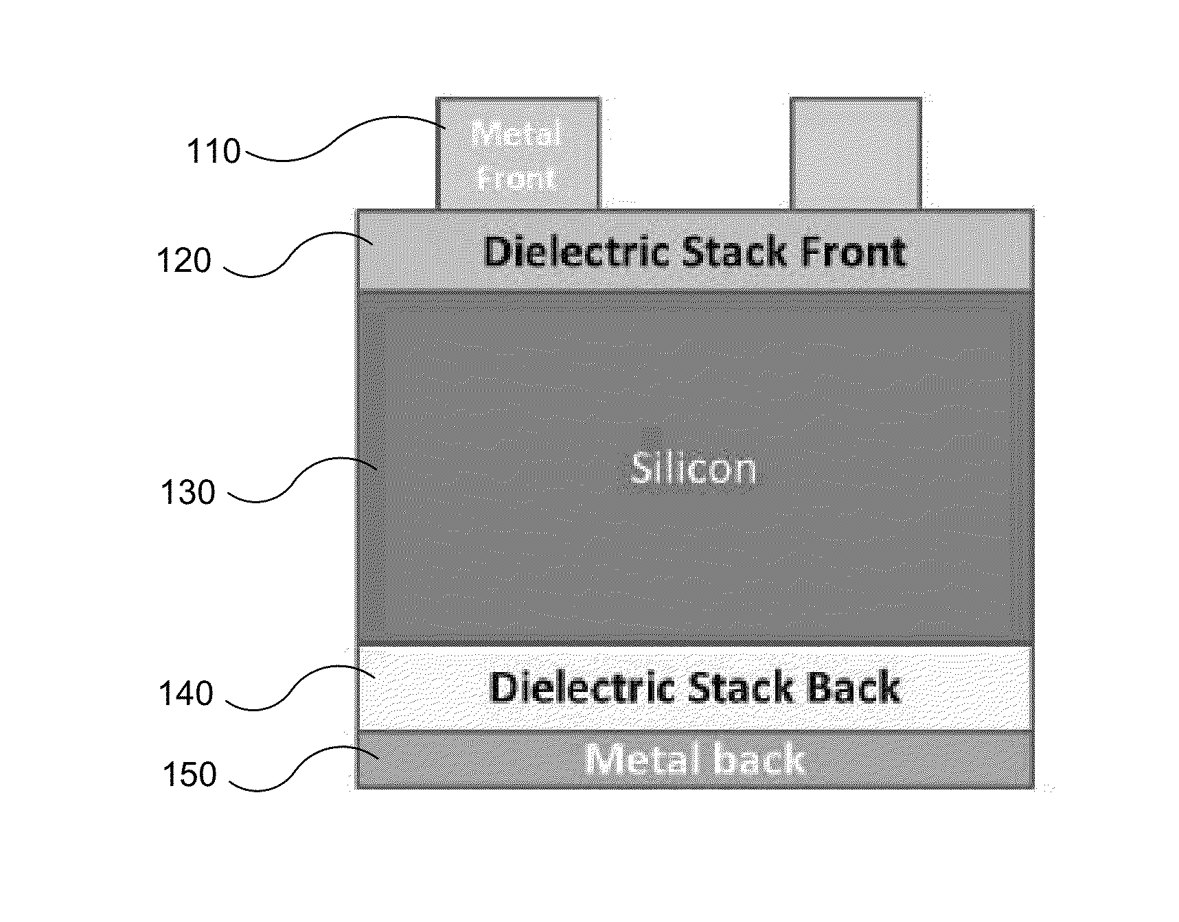
Dielectric-passivated metal insulator photovoltaic solar cells
a metal contact structure and photovoltaic solar cell technology, applied in the field of dielectric layers of solar cells, can solve the problems of loss of solar cell efficiency, high difficulty in fully reducing the recombination caused by using this type of metal contact structure, relative complexity and manufacturing cos
- Summary
- Abstract
- Description
- Claims
- Application Information
AI Technical Summary
Benefits of technology
Problems solved by technology
Method used
Image

Examples
Embodiment Construction
I. Solar Cell Overview and Benefits
[0017]Often, conventional and widely used solar cells use emitter structure to draw holes to p-type polarity and base structure electrons to n-type polarity. The “emitter structures” and the “base structures” may be composite structures which are accomplished using a series of processing steps which entail manufacturing higher doping areas, patterning, and achieving differential dopings—a complex fabrication process. In addition to the complexity, these generic structures may not be the best electrical performers for several reasons. First, the dopings under the contacts which may primarily serve the function of reducing contact resistance of majority carriers and increasing the contact rejection of the minority carriers may entail significant minority carrier loss because of its relative inefficiency at rejection. Second, these structures require raising the temperature of the wafer which in turn, has the risk of compromising the bulk lifetime of ...
PUM
 Abstract
Description
Claims
Application Information