
Photoresist and post etch residue cleaning solution

a technology of photoresist and residue, applied in the field of cleaning solution, can solve the problems of methylpyrrolidone (, inability to achieve complete removal of many dry-film resists, compatibility problems with photoresists, etc., and achieve the effect of effective simultaneously cleaning

Inactive Publication Date: 2015-05-14
DYNALOY
View PDF19 Cites 9 Cited by
  • Summary
  • Abstract
  • Description
  • Claims
  • Application Information

AI Technical Summary

Benefits of technology

The patent describes a new cleaning solution that can effectively clean both photoresist residues and post etch residues during a heating and cooling cycle. This solution is stable and reliable, making it a useful tool for semiconductor manufacturing processes.

Problems solved by technology

Similarly, compositions which use pyrrolidone-based solvents such as N-methylpyrrolidone (NMP) exhibit the same drawback in that they have not achieved complete removal of many dry-film resists and have compatibility problems with the photoresists.
In general, compositions which include a quaternary ammonium hydroxide as tetramethylammonium hydroxide (TMAH) in N-methyl pyrrolidone are not compatible with cured polyimide layers on the wafer.
A solution which is incompatible with the wafer features can result in further undesirably etching these metal surfaces including the copper pillars and solder bumps, resulting in yield loss.

Method used


Image

  • Photoresist and post etch residue cleaning solution
  • Photoresist and post etch residue cleaning solution
  • Photoresist and post etch residue cleaning solution

Examples


example 1

[0120]The components for the formulations tested, [1-8] in the following Examples were combined with stirring at room temperature to give between 100 and 300 g of a homogenous stripper solution. Solution homogeneity requires the KOH to be blended into the appropriate co-solvents prior to addition of DMSO. The surfactant is added into the blend last. The solution was heated to 93° C., with slow agitation for 2 hours. The timer was started when the solution reached the desired temperature. The solution was then removed from the heat source and left to cool to room temperature, 23° C. Observations about solution clarity and amount of precipitate were recorded in Table 2.

example 2

[0121]The components for the formulations tested in the following Examples were combined with stirring at room temperature to give between 100 and 300 g of a homogenous stripper solution. Solution homogeneity requires the KOH to be blended into the appropriate co-solvents prior to addition of DMSO. The surfactant is added into the blend last. The solution was heated to between 93° C., with slow agitation. Patterned test wafers with solder bumps positioned as an array in a polyimide film were obtained. The test wafers had been processed in a high energy oxidizing plasma to remove about 1-3 μm of polyimide. Residues deposited on the sides and tops of solder bumps during a plasma process were not removed prior to these tests. The patterned test wafers were cleaved into ˜4×3 cm pieces and mounted into a small scale wafer holder.

[0122]Unless otherwise noted in a Table, each stripper solution was heated to 93° C. and a wafer piece immersed. The timer was started as soon as they were fully...

example 3

[0125]The components for the formulations tested, [9-25] in the following Examples were combined with stirring at room temperature to give between 300 g of a homogenous stripper solution. Solution homogeneity requires the KOH to be blended into the appropriate co-solvents prior to addition of DMSO. The surfactant is added into the blend last. The solution was heated to 93° C., with slow agitation for 2 hours. 93° C. was selected as an extreme temperature to exacerbate any stability problems that could occur. The timer was started when the solution reached the desired temperature. The solution was then removed from the heat source and left to cool to room temperature, 23° C. Observations about solution clarity and amount of precipitate were recorded in Table 3.


PUM

PropertyMeasurementUnit
flash pointaaaaaaaaaa

Abstract

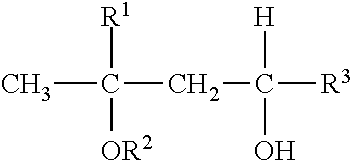
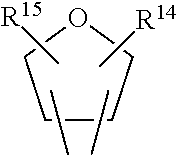
A process for cleaning a semi-conductor wafer comprising providing etched wafer containing metal pillars, contacting the etched wafer with a cleaning solution, removing the wafer from the cleaning solution, wherein the resulting wafer is substantially free of post etch residues and photoresist residues without etching the metal pillars by the cleaning solution, the cleaning solution comprising:A. a polar aprotic solvent,B. an inorganic base;C. a co-solvent for said inorganic base;D. a unsaturated cycloaliphatic compound having a ring ether group and at least one substituent bearing a primary hydroxyl group; andE. an organic base comprising an amine compound.The wafer containing photoresist residue or post etch residue can be cleaned by contacting the solution in a spray or immersion.

Description

1. CROSS-REFERENCE TO RELATED APPLICATION[0001]This application is a divisional of U.S. application Ser. No. 13 / 651,790 filed on Oct. 15, 2012, which claims priority to U.S. Provisional Application Ser. No. 61 / 557,229 filed Nov. 8, 2011, the disclosures of which are incorporated herein by reference in its entirety.2. FIELD OF THE INVENTION[0002]The present disclosure relates to a cleaning solution for removing residues from semiconductor substrates, and particularly to remove post etch residues from wafers.3. BACKGROUND OF THE INVENTION[0003]The technology of fabricating semiconductor integrated circuits has advanced with regard to the number of transistors, capacitors and other electronic devices which can be fabricated on a single integrated circuit chip. This increasing level of integration has resulted in large part from a reduction in the minimum feature sizes of the integrated circuits and an increase in the number of layers and functionality which make up the integrated circu...

Claims


Application Information

Patent Timeline
Patent Type & Authority Applications(United States)
IPC IPC(8): C11D11/00C11D3/43H01L21/02C11D3/30C11D3/20C11D3/04C11D1/72C11D3/34
CPCC11D11/0047C11D1/72C11D3/43C11D3/3445H01L21/02041C11D3/2068C11D3/044C11D3/2096C11D3/30G03F7/426G03F7/425C11D2111/22C11D3/2024
Inventor POLLARD, KIMBERLY DONAPFETTSCHER, DONALD JAMESHATFIELD, MEAGANHOCHSTETLER, SPENCER ERICHGILBERT, NICHELLE MARIAPHENIS, MICHAEL TOD
Owner DYNALOY
Learn More