Semiconductor device and method for manufacturing the same

a technology of semiconductors and semiconductors, applied in semiconductor devices, electrical devices, transistors, etc., can solve the problems of high surge voltage or oscillation, vacancy-oxide-hydrogen (voh) defect, and the inability to disclose a method for reducing crystal defects caused, so as to suppress the oscillation of voltage and current, suppress the spreading of a depletion layer, and reduce the effect of generation loss

Active Publication Date: 2015-06-25
FUJI ELECTRIC CO LTD
View PDF13 Cites 39 Cited by
  • Summary
  • Abstract
  • Description
  • Claims
  • Application Information

AI Technical Summary

Benefits of technology

[0042]According to the semiconductor device and the semiconductor device manufacturing method of the invention, it is possible to suppress the spreading of a depletion layer, to ensure a breakdown voltage, to reduce generation loss, and to suppress the oscillation of voltage and current during a switching operation. In addition, according to the semiconductor device and the semiconductor device manufacturing method of the invention, it is possible to recover a crystal defect to reduce a leakage current and to reduce the risk of thermal runaway due to a high-temperature operation.

Problems solved by technology

As a result, a vacancy-oxide-hydrogen (VOH) defect occurs.
However, it does not disclose a method for reducing crystal defects caused by proton implantation.
As a result, the concentration of holes, which are minority carriers, is significantly reduced and the holes are quickly depleted during reverse recovery, which results in a high surge voltage or oscillation.
When the acceleration energy increases, a defect occurs in a crystal due to implantation damage.
The oscillation is radiated as radiation noise to the outside and causes an electro-magnetic compatibility (EMC) problem.

Method used


Image

  • Semiconductor device and method for manufacturing the same
  • Semiconductor device and method for manufacturing the same
  • Semiconductor device and method for manufacturing the same

Examples


example 1

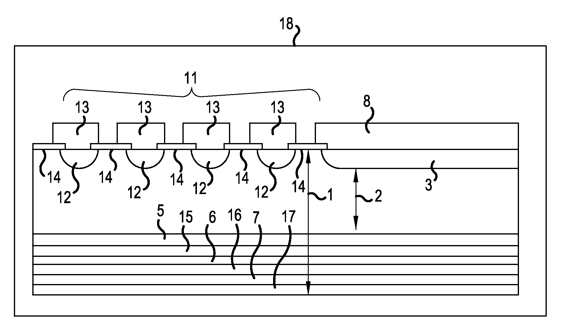
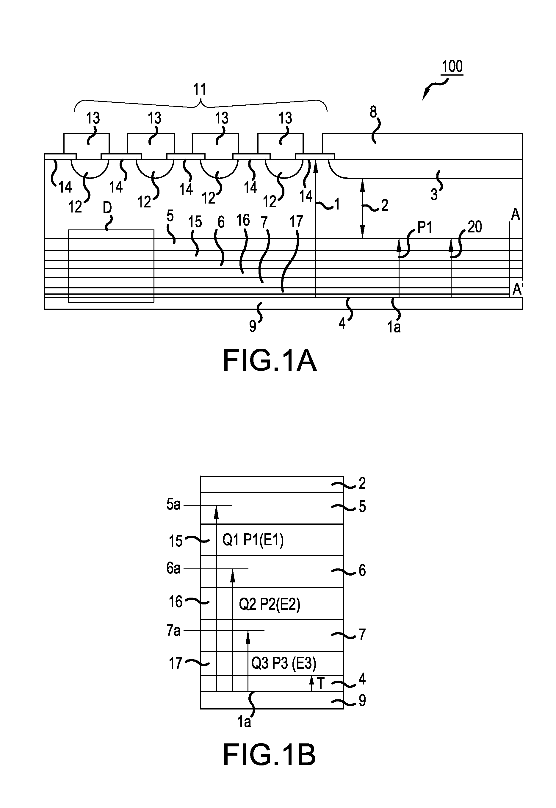
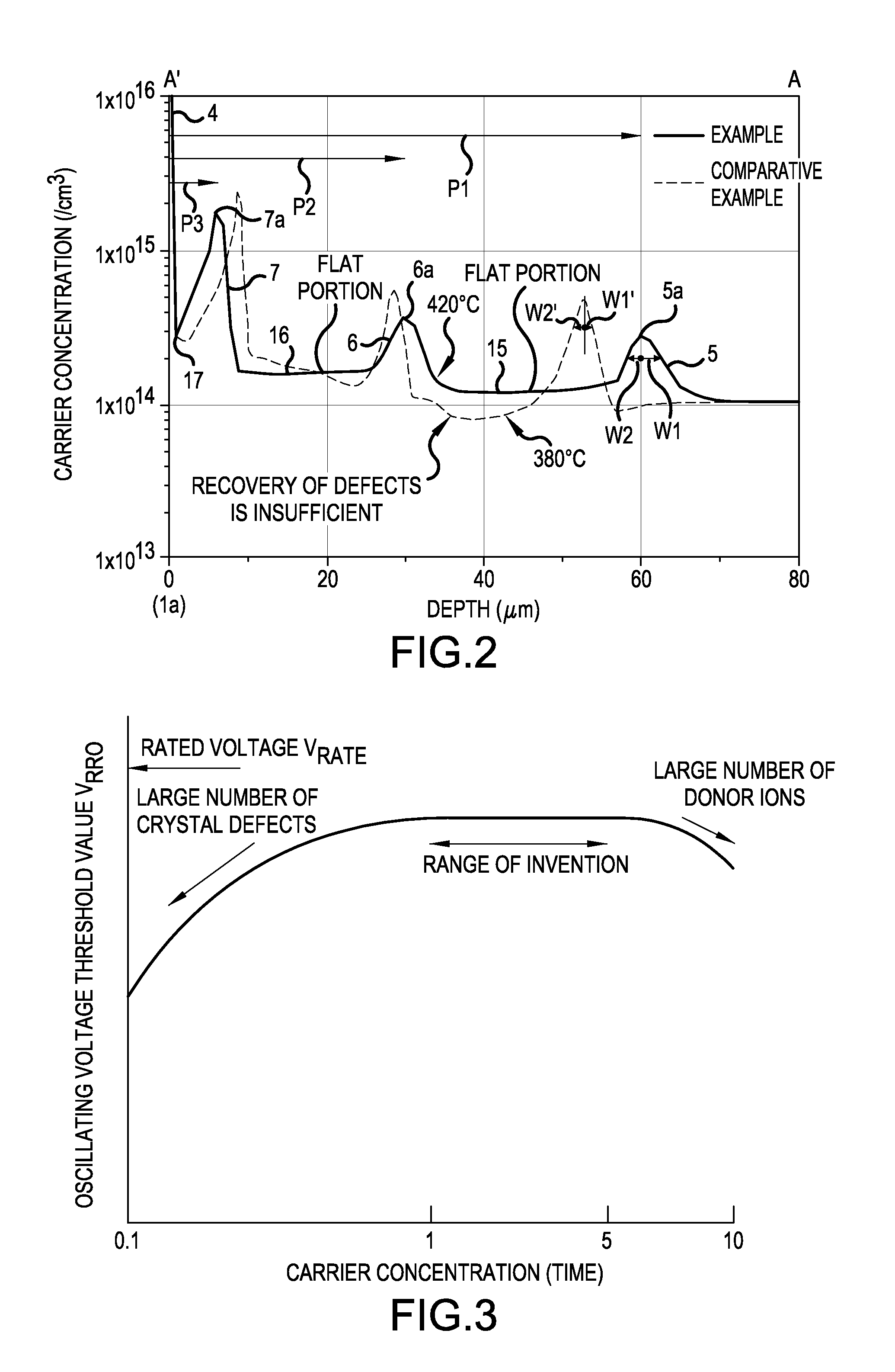
[0061]The structure of a semiconductor device according to Example 1 will be described. FIGS. 1A and 1B are cross-sectional views illustrating the structure of the semiconductor device according to Example 1 of the invention. FIG. 1A is a cross-sectional view illustrating a main portion and FIG. 1B is an enlarged view illustrating a portion D. FIG. 1B illustrates the depth of n-type buffer layers 5, 6, and 7. A PiN diode 100 is given as an example of the semiconductor device according to Example 1 illustrated in FIGS. 1A and 1B. The PiN diode 100 has a breakdown voltage of 1200 V. The following carrier concentration is calculated from spreading resistance (SR).

[0062]The PiN diode 100 includes a p-type anode layer 3 that is provided in a surface layer of a first main surface (front surface) of an n-type silicon substrate 1 with a thickness of about 120 μm and an n-type cathode layer 4 which is provided in a second main surface (rear surface). Three n-type buffer layers 5, 6, and 7 ar...

example 2

[0099]Next, a method for manufacturing the semiconductor device illustrated in FIGS. 1A and 1B will be described as Example 2. FIGS. 4 to 7 are cross-sectional views illustrating the state of the semiconductor device according to Example 2 of the invention which is being manufactured. First, as illustrated in FIG. 4, for example, the p-type anode layer 3 and the p-type layer 12 of the high-breakdown-voltage junction termination structure 11 are selectively formed in a surface layer of one main surface of the n-type silicon substrate 1 with a thickness of about 500 μm. Then, the insulating film 14, which is an oxide film, is formed on the surface of a region of the n-type silicon substrate 1 which is interposed between the p-type anode layer 3 and the p-type layer 12 and on the surface of a region interposed between the p-type layers 12. Then, the anode electrode 8 is formed on the p-type anode layer 3 and the termination electrode 13 is formed on the p-type layer 12. Then, the other...

example 3

[0116]Next, the structure of an insulated gate bipolar transistor (IGBT) will be described as an example of the structure of a semiconductor device according to Example 3 of the invention. FIGS. 12A and 12B are diagrams illustrating the structure of the semiconductor device according to Example 3 of the invention. FIG. 12A is a cross-sectional view illustrating a main portion of the semiconductor device according to Example 3. FIG. 12B illustrates a net doping concentration distribution along the cutting line A-A′ of FIG. 12A.

[0117]As illustrated in FIGS. 12A and 12B, an n− drift layer 2 which is an n− semiconductor substrate is provided and a p-type base layer 33 which has a higher impurity concentration than the n− drift layer 2 is provided in a surface layer of a front surface of the n− semiconductor substrate. An n+ emitter layer 34 which has a higher impurity concentration than the p-type base layer 33 is provided in the p-type base layer 33. A gate electrode 42 is formed so as...


PUM


Abstract

A semiconductor device is disclosed in which proton implantation is performed a plurality of times to form a plurality of n-type buffer layers in an n-type drift layer at different depths from a rear surface of a substrate. The depth of the n-type buffer layer, which is provided at the deepest position from the rear surface of the substrate, from the rear surface of the substrate is more than 15 μm. The temperature of a heat treatment which is performed in order to change a proton into a donor and to recover a crystal defect after the proton implantation is equal to or higher than 400° C. In a carrier concentration distribution of the n-type buffer layer, a width from the peak position of carrier concentration to an anode is more than a width from the peak position to a cathode.

Description

BACKGROUND OF THE INVENTION[0001]A. Field of the Invention[0002]The present invention relates to a semiconductor device, such as a p-intrinsic-n (PiN) diode or an insulated gate bipolar transistor (IGBT) including a buffer layer formed by proton implantation, and a method for manufacturing the same.[0003]B. Description of the Related Art[0004]Examples of a power semiconductor device include a diode or an IGBT with a breakdown voltage of 400 V, 600 V, 1200 V, 1700 V, 3300 V, or more. The diode or the IGBT is used in a power conversion device such as a converter or an inverter. The power semiconductor device requires low loss, low noise, a high breakdown voltage, and low cost.[0005]FIG. 8 is a cross-sectional view illustrating a main portion of a PiN diode 500 including a general n-type buffer layer 55. As illustrated in FIG. 8, the PiN diode 500 includes an n-type drift layer 52 which is a portion of an n-type silicon substrate 51. A p-type layer, which will be a p-type anode layer 5...

Claims


Application Information

Patent Timeline
Patent Type & Authority Applications(United States)
IPC IPC(8): H01L21/02H01L29/739H01L29/66H01L29/868
CPCH01L21/02351H01L29/868H01L21/02304H01L29/66333H01L29/7395H01L21/263H01L29/0619H01L29/1095H01L29/32H01L29/36H01L29/365H01L29/66136H01L29/66348H01L29/7397H01L29/8611H01L29/402H01L29/404H01L29/167
Inventor ONOZAWA, YUICHI
Owner FUJI ELECTRIC CO LTD
Why Eureka
Try Eureka