

Composite Structure for Gate Level Inter-Layer Dielectric
a dielectric and gate-level technology, applied in the direction of semiconductor devices, electrical apparatus, transistors, etc., can solve the problems of shifting the work function of the electrode metal, adversely affecting the suitability of the gate electrode,
- Summary
- Abstract
- Description
- Claims
- Application Information
AI Technical Summary
Benefits of technology
Problems solved by technology
Method used
Image

Examples
Embodiment Construction
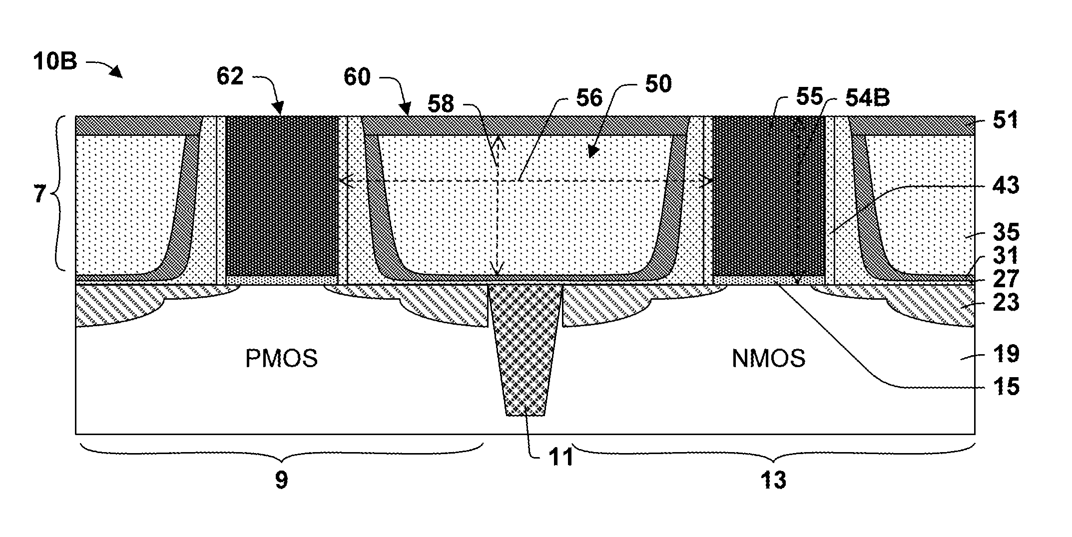
[0007]It has been observed that gate height may be unintentionally reduced through the dummy gate removal process and that this can have an adverse effect on device performance. The present disclosure solves this problem by forming the inter-level dielectric at the gate level (ILD0) to be a composite of two or more layers, with the upper layer having a higher resistance to the etch process used for dummy gate removal. The composite ILD0 better maintains gate height through the gate replacement process and provides integrated circuit devices having metal gates with a more easily predetermined and consistent height.
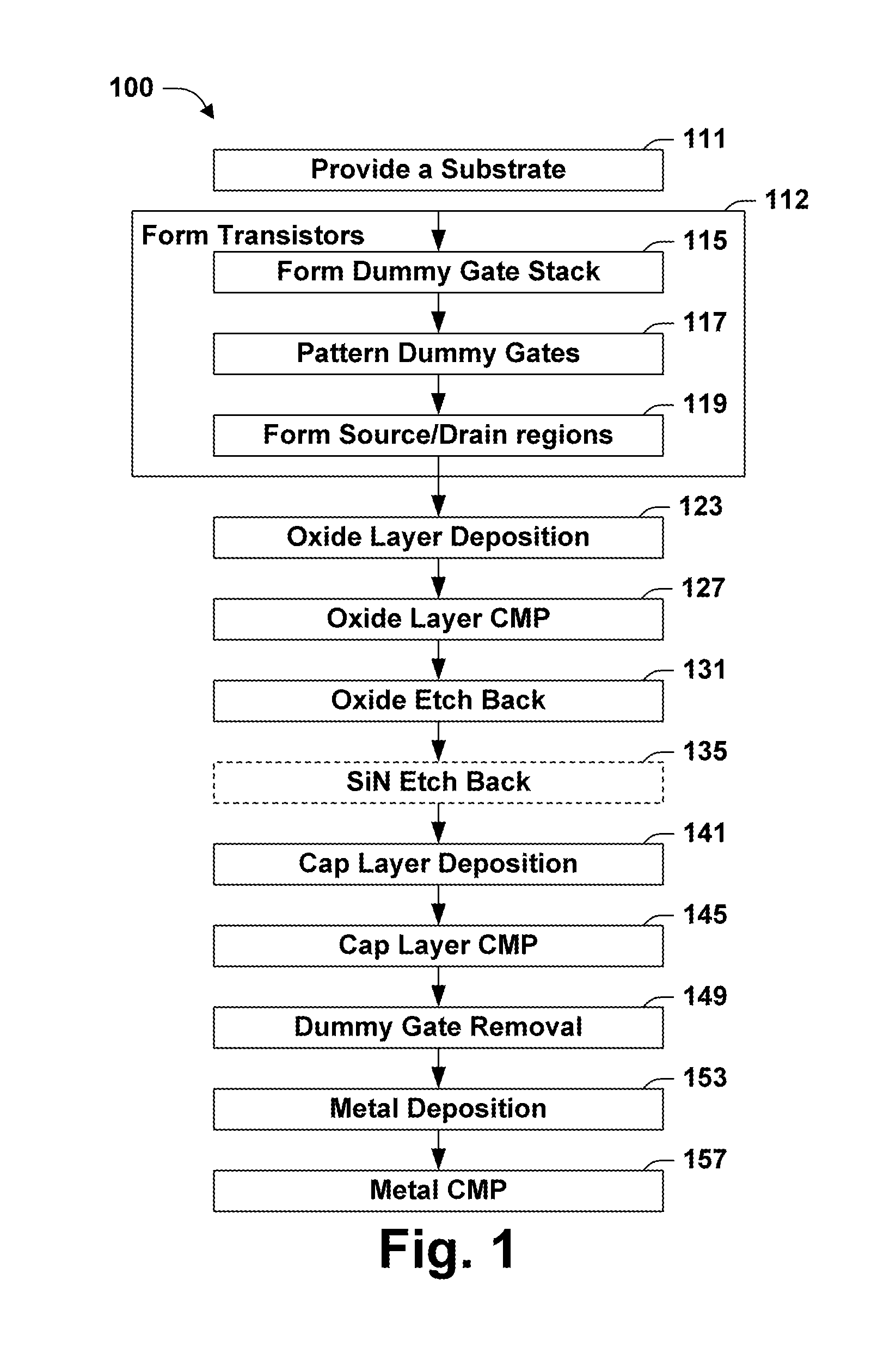
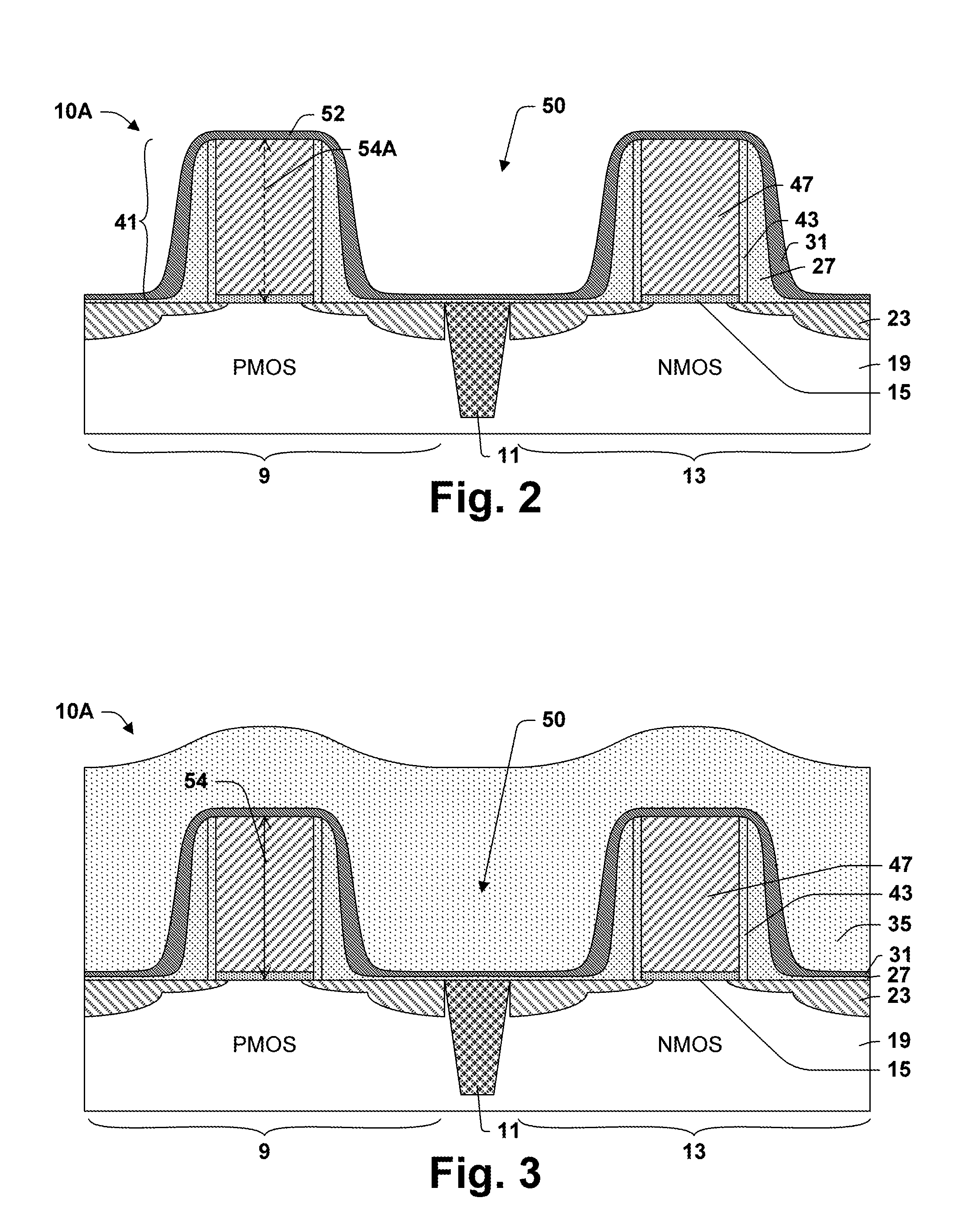
[0008]FIG. 1 provides a flow chart of a process 100 that is an example of one group of embodiments provided by the present disclosure. FIGS. 2-11 illustrate an integrated circuit device 10A, an example according to another embodiment of the present disclosure, as it undergoes manufacture by process 100. FIGS. 12-13 illustrate an integrated circuit device 10B, an example acc...
PUM
 Abstract
Description
Claims
Application Information