
Capacitors Including Inner and Outer Electrodes

a technology of capacitors and electrodes, applied in the direction of capacitors, semiconductor devices, electrical apparatus, etc., can solve the problems of increasing leakage, increasing leakage, and increasing the thickness of the electrode, so as to reduce the leakage of the first layer

Inactive Publication Date: 2015-07-02
INTERMOLECULAR
View PDF9 Cites 10 Cited by
  • Summary
  • Abstract
  • Description
  • Claims
  • Application Information

AI Technical Summary

Benefits of technology

The patent relates to a capacitor structure that includes a negative inner electrode and a dielectric layer. The first layer is made of a chemically stable or weakly unstable material that directly interfaces with the second layer. This material has a low instability energy with the second layer material. The electron affinity of the first layer material is also lower than that of the second layer material to minimize leakage. Technical effects include improved performance and reliability of the capacitor structure.

Problems solved by technology

The lower barrier height leads to increased leakage, which undesirable for many applications that, for example, require preservation of the charge for prolonged periods of time.
Furthermore, the small thickness also increases leakage due to direct tunneling.
However, most of the high work function materials are very expensive and / or difficult to deposit.
Specifically, use of these materials has led to various deposition problems in a typical DRAM geometry.
By way of example, silicon is not chemically stable in contact with most high-k materials and may produce layers of silicon oxide.
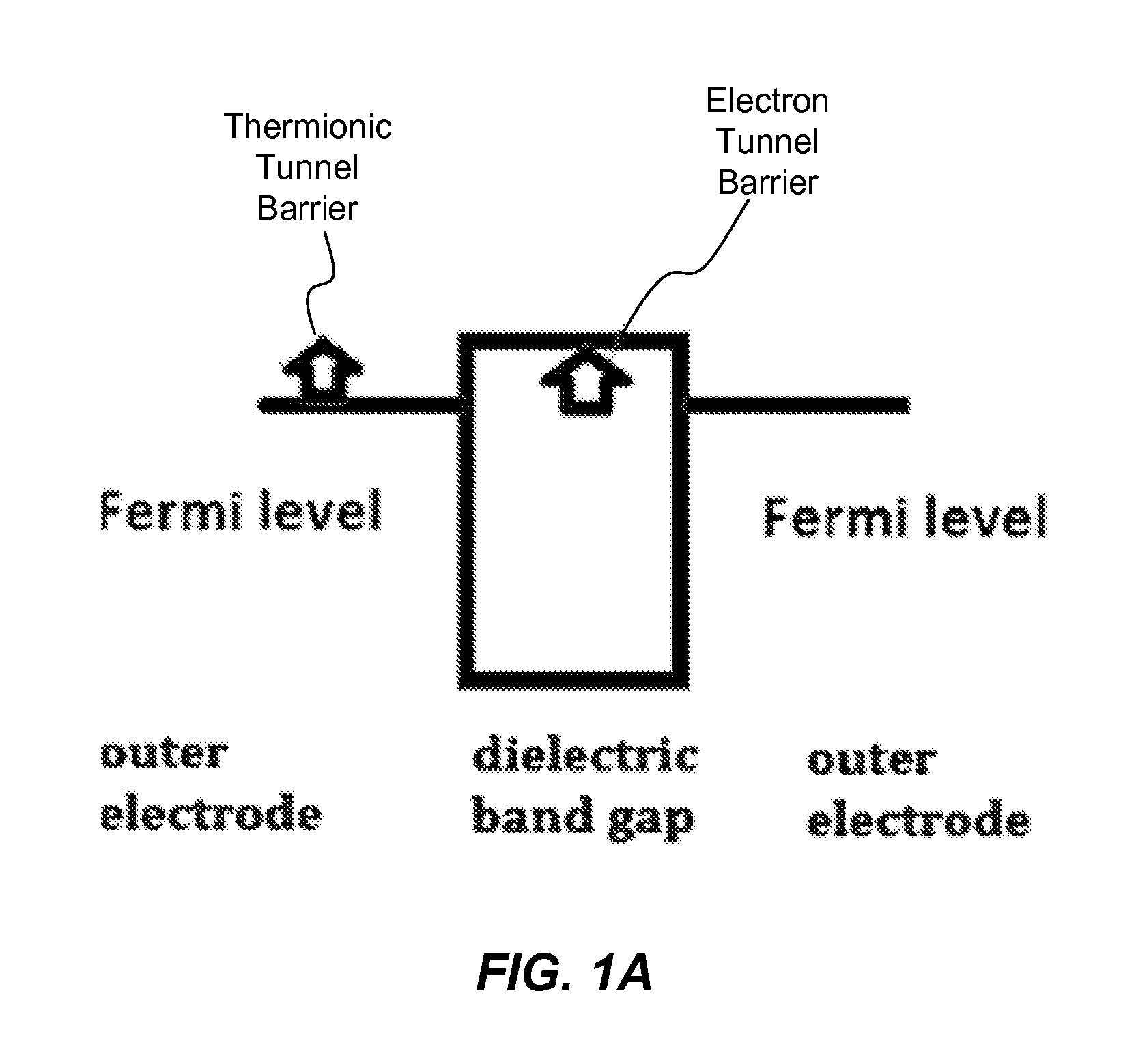
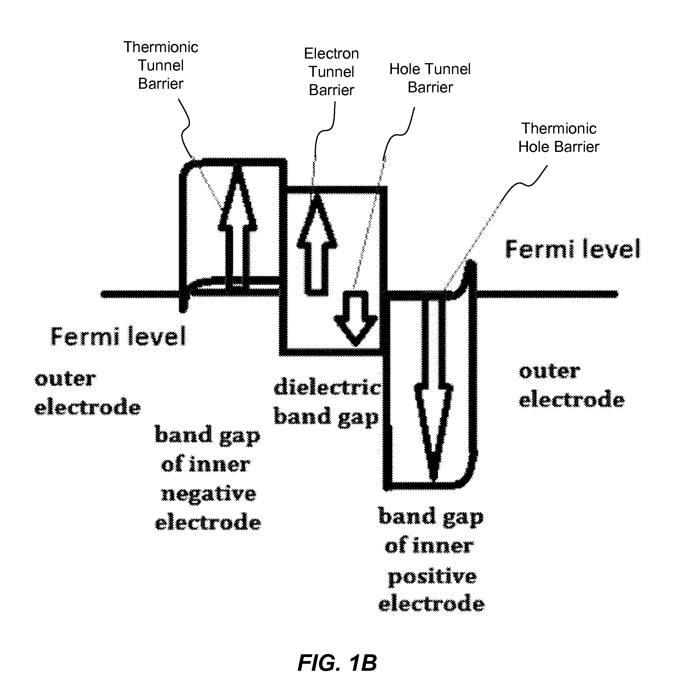
Disparity of work functions at different electrodes may create built-in fields that would partially deplete the inner negative electrode and would decrease the effective tunneling barrier.
For example, doped silicon, while possessing many electrical characteristics presented above, may not be an advantageous inner electrode to use with a titanium oxide dielectric.
Doped silicon may be similarly unstable when interfacing zirconium oxide.
In some embodiments, the material of an inner electrode may be “weakly unstable;” not stable in the very strictest sense, yet stable enough for use in these devices, when in contact with the material of the dielectric layer.
For example, GaAs can be heavily p-doped and is chemically stable when interfacing zirconium oxide ZrO2, however the electron affinity of GaAs is not sufficiently small compared to the electron affinity of ZrO2.

Method used


Image

  • Capacitors Including Inner and Outer Electrodes
  • Capacitors Including Inner and Outer Electrodes
  • Capacitors Including Inner and Outer Electrodes

Examples


application examples

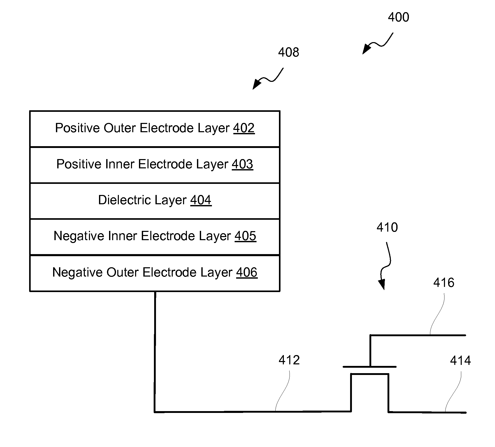
[0053]Examples of applications for capacitor stacks include DRAM devices. DRAM memory cells effectively use a capacitor to store charge for a period of time, with the charge being electronically “read” to determine whether a logical “one” or “zero” has been stored in the associated cell. A cell transistor may be used to access the cell. The cell transistor is turned “on” in order to store data on each associated capacitor and is otherwise turned “off” to isolate the capacitor and preserve its charge. More complex DRAM cell structures exist, but this basic DRAM structure will be used for illustrating the application of this disclosure to DRAM devices.

[0054]FIG. 4 is a schematic illustration of a DRAM device 400 including a capacitor stack 408 and a transistor 410. DRAM device 400 may be also referred to as a DRAM cell, while capacitor stack 408 may be also referred to a cell capacitor, and transistor 410 may be referred to as a cell transistor. Transistor 410 may be a MOS transistor ...


PUM


Abstract

Provided are capacitor stacks for use in integrated circuits and methods of fabricating these stacks. A capacitor stack includes a dielectric layer and one or two inner electrode layers, such as a positive inner electrode layer and a negative inner electrode layer. The inner electrode layers directly interface the dielectric layer. The stack may also include outer electrode layers. The inner electrode layers are either chemically stable or weakly chemically unstable, while in contact with the dielectric layer based on the respective phase diagrams. Furthermore, the electron affinity of the positive inner electrode layer may be less than the electron affinity of the dielectric layer. The sum of the electron affinity and bandgap of the negative inner electrode layer may be less than that of the dielectric layer. In some embodiments, inner electrode layers are formed from heavily doped semiconducting materials, such as gallium arsenide or gallium aluminum arsenide.

Description

BACKGROUND[0001]Dynamic Random Access Memory utilizes capacitors to store bits of information within an integrated circuit. Capacitors are also commonly used in other electronic devices.[0002]A capacitor is formed by placing a dielectric material between two electrodes formed from conductive materials. A capacitor's ability to hold electrical charge (i.e., capacitance) is a function of the surface area of the capacitor plates A, the distance between the capacitor plates d (i.e. the physical thickness of the dielectric layer), and the relative dielectric constant or k-value of the dielectric material. The capacitance is given by:C=kɛoAd(Eqn.1)where ∈0 represents the vacuum permittivity.[0003]The dielectric constant is a measure of a material's polarizability. Therefore, the higher the dielectric constant of a material, the more charge the capacitor can hold. Therefore, if the k-value of the dielectric is increased, the area of the capacitor can be decreased and maintain the desired c...

Claims


Application Information

Patent Timeline
Patent Type & Authority Applications(United States)
IPC IPC(8): H01L49/02H10N97/00
CPCH01L28/75H01L29/66181H01L29/94H10B12/03
Inventor BARABASH, SERGEYPRAMANIK, DIPANKAR
Owner INTERMOLECULAR
Learn More