Metal-insulator-metal waveguide for nano-lasers and optical amplifiers

a technology of metal-insulator metal and nano-lasers, applied in the direction of lasers, fiber transmission, transmission, etc., can solve the problems of high optical loss, difficult to make direct electrical contacts with the confining metal, and high optical loss of metal mirrors, so as to achieve great control over size, shape and position.

Inactive Publication Date: 2015-07-02
HILL MARTIN TERENCE
View PDF5 Cites 9 Cited by
  • Summary
  • Abstract
  • Description
  • Claims
  • Application Information

AI Technical Summary

Benefits of technology

[0047]Typically selective wet chemical processes of either etching or oxidization are used to remove the semiconductor core material under the second metal layer and n-InP layer, starting from the sides, and replace it with the low refractive index material. Preferably removal of the semiconductor core material progresses uniformly from each side, leaving a section of semiconductor core material in the centre of the waveguide structure below a plateau of the second metal layer and n-InP layer. Advantageously by controlling the etch time, and also the shape of the edges of the etch mask used to transfer the etch mask pattern isotropically into the wafer, great control over the size, shape and position of the semiconductor core material in the centre of the waveguide structure can be achieved. Typically the etching processes used to remove or replace the semiconductor core material can to some extent be used to transfer the pattern of the InP layer at the edge of the waveguide into the semiconductor core material that remains in the centre of the waveguide structure.

Problems solved by technology

Unfortunately, the metal conduction electrons which oscillate in synchronism with the optical field dissipate energy through collisions with the metal's atomic lattice.
This energy dissipation leads to high optical losses, so SPPs can only travel short distances and metal mirrors have higher losses than dielectric ones.
For shorter wavelengths, and when the size of the semiconductor region is to be reduced down to a thickness of a few hundred nanometres or less, then this simple approach of making direct electrical contacts to the semiconductor with the confining metal becomes problematic.
The problems arise due to the following factors: adhesive metals such as titanium introduce significant optical losses at these shorter wavelengths and so, are difficult to employ.
However, as the active region in this particular structure is reduced in size, limitations in the approach appear.
The high gains required for the smaller widths would be difficult to achieve with semiconductor gain materials.
Thus for smaller widths, this waveguide concept is not suitable for lasers or amplifiers.
The key problem with this prior art waveguide design [1],[2],[3],[4] is that as the width of the waveguide is reduced, the energy of the mode goes into the dielectric layer and is poorly confined on the InGaAs region.

Method used


Image

  • Metal-insulator-metal waveguide for nano-lasers and optical amplifiers
  • Metal-insulator-metal waveguide for nano-lasers and optical amplifiers
  • Metal-insulator-metal waveguide for nano-lasers and optical amplifiers

Examples


first embodiment

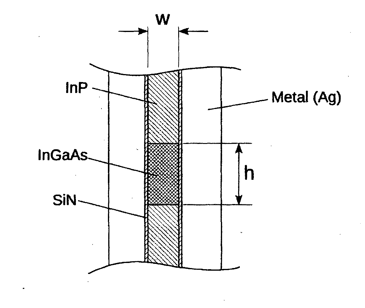
[0064]an improved MIM waveguide structure 10 in accordance with the invention, as illustrated in FIG. 5, comprises a substrate 12 on which are supported first and second metal layers 14 and 16 which form electrical contacts for the waveguide. A narrow ridge of low-band gap semiconductor core 18, which forms the optical gain material, is sandwiched between the two metal layers 14 and 16. The semiconductor core 18 is surrounded on both sides by a low refractive index material 19 which is also sandwiched between the two metal layers 14 and 16. First and second layers of thin higher-band gap doped semiconductor material 15 and 17 are provided between the respective first and second metal layers 14 and 16 and the low-band gap semiconductor core 18. The improved MIM waveguide structure still provides an electrical path to the optical gain medium via the thin higher-band gap doped semiconductor layers 15 and 17. The optical mode that propagates down this waveguide is localised in the centr...

second embodiment

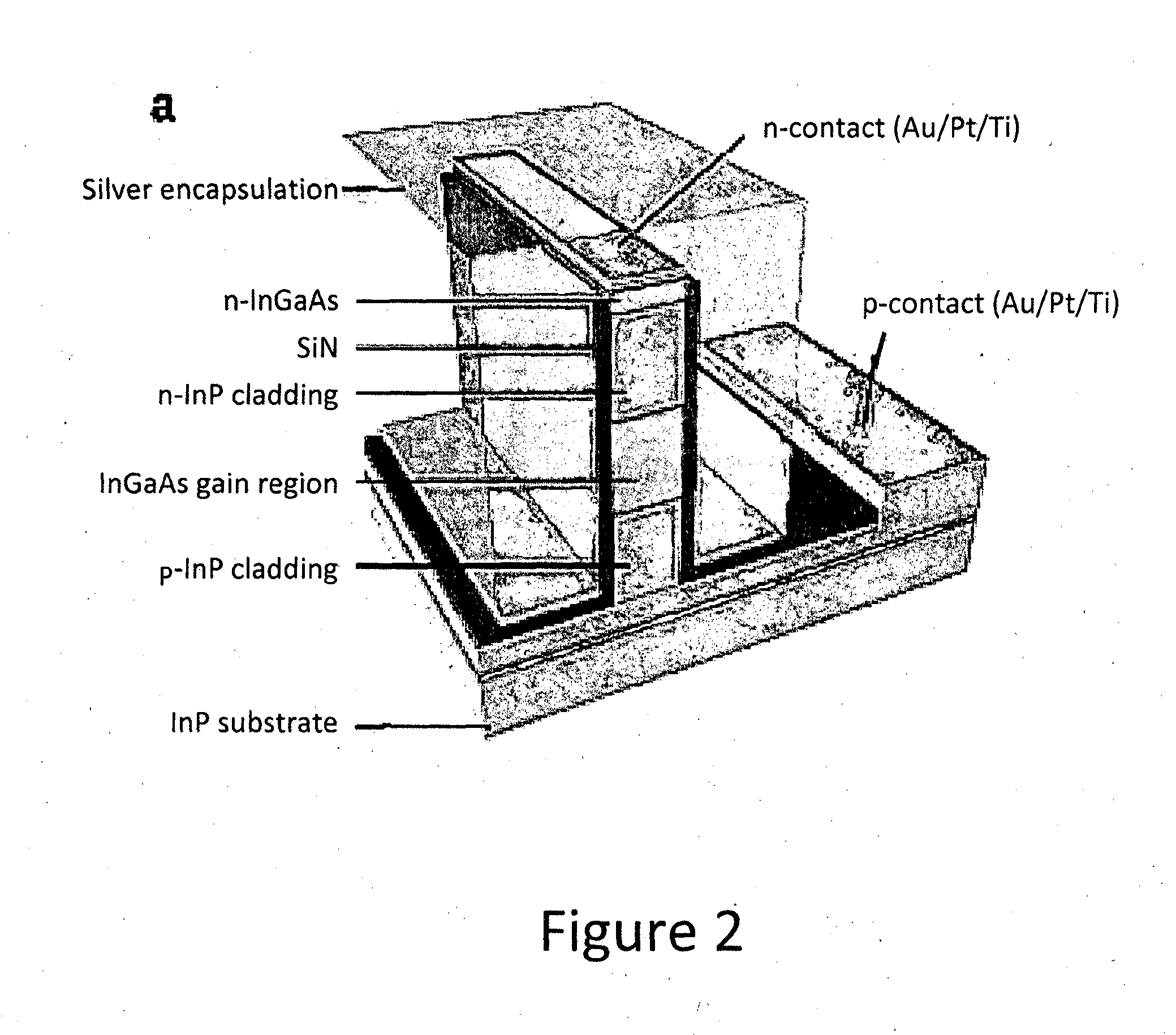
[0086]FIG. 10 shows a cross-section of a waveguide structure 60 with a series of such thin sections 62 of low band-gap semiconductor core material in the middle of the waveguide. In the epitaxial growth process the semiconductor core material could be grown out of a number of layers of semiconductors of various compositions. Here a number of layers 62 of InGaAs low band-gap semiconductor core material are shown separated by thin InP layers 64. The height of the low-band gap sections 62 in the core of the waveguide can be made small enough so that quantum confinement effects are seen, to improve the performance of the devices. For wide gain regions, (greater than say 30 nm wide) the gain material will look like multi-quantum well gain material, which can have significant performance improvements compared to bulk semiconductor.

[0087]When the width of the gain region is made small (less than approximately 30 nm) the quantum confinement effects may occur in two dimensions. In this case ...


PUM

PropertyMeasurementUnit
optical wavelengthsaaaaaaaaaa
refractive indexaaaaaaaaaa

Abstract

A metal-insulator-metal (MIM) waveguide structure for nano-lasers or optical amplifiers is described. The structure comprises a substrate on which are supported first and second metal layers which form electrical contacts for the waveguide. A narrow ridge of low-band gap semiconductor core, which forms the optical gain material, is sandwiched between the two metal layers. The semiconductor core is surrounded on both sides by a low refractive index material which is also sandwiched between the two metal layers. First and second layers of thin higher-band gap doped semiconductor material are provided between the respective first and second metal layers and the low-band gap semiconductor core and the low refractive index material. The optical mode that propagates down this waveguide is localised in the centre of the waveguide structure where the narrow ridge of low-band gap semiconductor core is.

Description

FIELD OF THE INVENTION[0001]The present invention relates to the improved design of a metal-insulator-metal (MIM) waveguide structure and a method of manufacture of the same and relates particularly, though not exclusively, to metallic / plasmonic nano-lasers and optical amplifiers based on such a MIM waveguide structure.BACKGROUND TO THE INVENTION[0002]Reducing the size of lasers and other photonic devices produces benefits similar to those seen with the shrinking dimensions of electronic components. A smaller laser requires less power and can potentially be switched on and off faster. In theory it is possible to use metals to form the laser resonator. The metal may form either strong compact mirrors, able to confine light to about the size of the diffraction limit. Alternatively, the light may interact strongly with the free electrons in the metal, being guided in the form of surface plasmon polaritons (SPPs) at the interface between a metal (conductor) and a dielectric (non-conduct...

Claims


Application Information

Patent Timeline
Patent Type & Authority Applications(United States)
IPC IPC(8): H01S3/067G02F1/017
CPCH01S3/06708G02F1/01708H01S3/06754H01S5/1046H01S5/1064H01S5/3412H01S5/2205H01S5/2213B82Y20/00H01S5/04252
Inventor HILL, MARTIN TERENCE
Owner HILL MARTIN TERENCE
Why Eureka
Try Eureka