Pattern inspection device and pattern inspection method

a technology of inspection device and pattern, which is applied in the direction of material analysis using wave/particle radiation, photomechanical equipment, instruments, etc., can solve the problems of increasing the frequency of systematic defects, deviation of line width from design value or tip shape, and increasing the difficulty of forming a pattern on a wafer as designed, so as to achieve accurate simulation of electron beam image and high-accuracy defect detection

Active Publication Date: 2015-07-30
HITACHI HIGH-TECH CORP
View PDF2 Cites 27 Cited by
  • Summary
  • Abstract
  • Description
  • Claims
  • Application Information

AI Technical Summary

Benefits of technology

[0008]According to the present invention, there is provided a pattern inspection device and a pattern inspection method for accurately simulating the electron beam image of a resist pattern on a wafer from design data and for implementing high-accuracy defect detection by comparing the simulated data and the real image.

Problems solved by technology

As a semiconductor circuit pattern becomes more and more miniaturized, the resolution of an exposure device is approaching the limit, making it more and more difficult to form a pattern on a wafer as designed.
The generation frequency of systematic defects, such as a line width deviation from a design value or a deformed tip shape, increases.
Because these systematic defects are generated in any of all dies, it is difficult to detect them in the conventional die-to-die (or abbreviated to D2D) inspection that compares between the data on the neighboring dies.

Method used


Image

  • Pattern inspection device and pattern inspection method
  • Pattern inspection device and pattern inspection method
  • Pattern inspection device and pattern inspection method

Examples


first embodiment

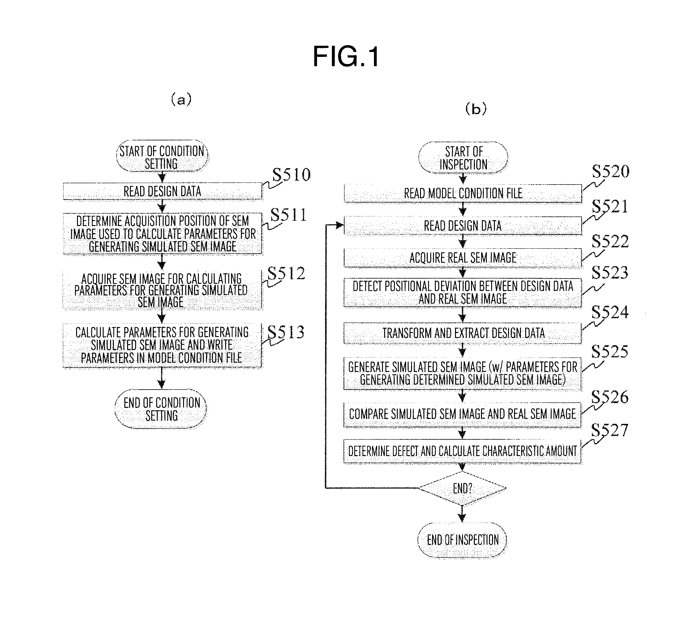
[0043]The following describes an overall configuration of a first embodiment of the present invention, followed sequentially by the description of the content of each processing.

(1-1) Overall Flow

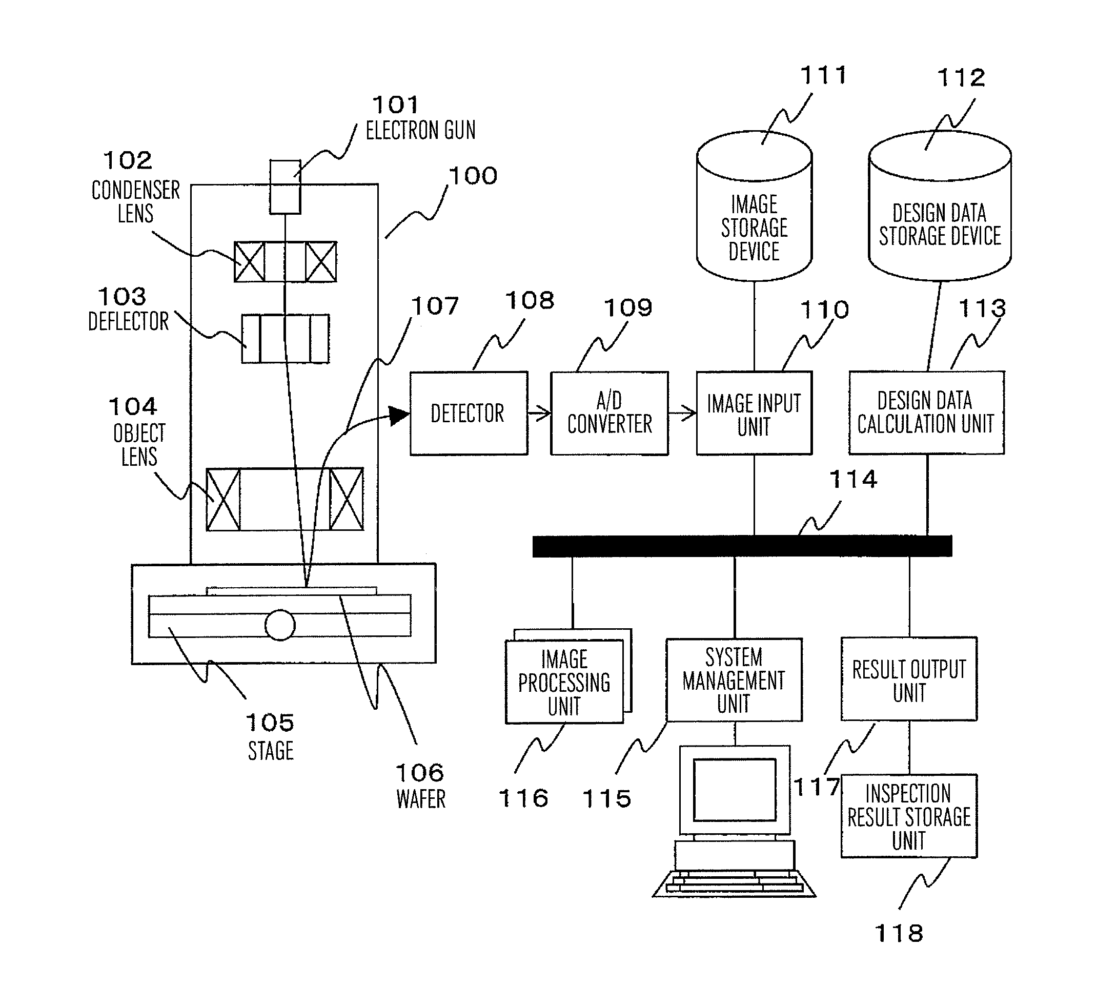
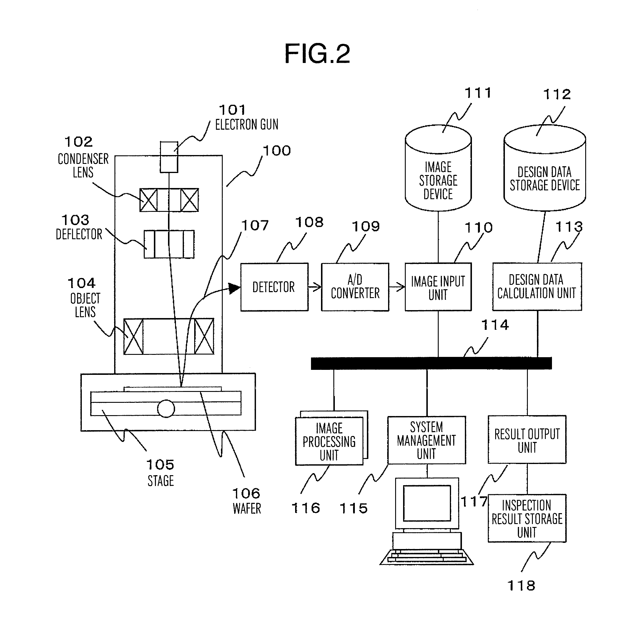
[0044]First, with reference to FIG. 2, the overall configuration of a pattern inspection device according to the present invention is described.

[0045]In this embodiment, a wafer image to be inspected is acquired by a scanning electron microscope (SEM). An electron optics system 100 includes an electron source 101 that generates an electron beam, a condenser lens 102 that converges the electron beam, a deflector 103 that deflects the electron beam into the XY direction, an object lens 104, and an XY stage 105. A secondary electron 107 generated from a wafer 106 is detected by a detector 108, is converted from the analog signal to the digital signal by an A / D converter 109, is input to an image input unit 110, and is stored in a storage device 111.

[0046]An image to be inspected is one of the ...

second embodiment

[0088]A second embodiment is an embodiment in which other types of design data are used. FIG. 17 shows the variations of design data. FIG. 17(a) shows a design intent, (b) shows a mask pattern, (c) shows a lithography simulation result with a mask pattern as its input, and (d) shows a contour line based on a lithography simulation result.

[0089]Although not specifically mentioned, (d) is used in the first embodiment. Of the remaining (a), (b), and (c), (c) represents multivalued data. The amount of multivalued data is so large that few inspection device users save the data of the whole inspection area in this format. Therefore, in the second embodiment, the case in which (a) is used and the case in which (b) is used are described. (d) has a shape similar to that of a real pattern on a wafer, while the deviation of (a) and (b) from a real pattern is so large that the preprocessing is required in each case to convert the shape.

[0090]First, FIG. 18 shows the preprocessing that is perfor...

third embodiment

[0094]FIG. 21 shows a third embodiment. The flow in FIG. 21 is similar to the flow in FIG. 3 in the first embodiment except that there is a plurality of simulated SEM images.

[0095]The reading of design data (S230), the reading of a SEM image (S231), the detection of a positional deviation (S232), and distortion correction and extraction (S233) are the same as those in the first embodiment. When generating a simulated SEM image in step S234, a plurality of simulated SEM images, different with each other in the pattern width (horizontal axis in the figure) and in the edge width (vertical axis in the figure, w in FIG. 7(b)), is generated. The image comparison (S235) is performed with the plurality of simulated SEM images and, only when a defect is detected in all comparisons, the defect information is output. In other words, if no defect is detected in at least one comparison, no defect information is output.

[0096]This method allows for a variation in the semiconductor process. That is...


PUM

PropertyMeasurementUnit
electron beamaaaaaaaaaa
electron beam imageaaaaaaaaaa
shapeaaaaaaaaaa

Abstract

Provided is a pattern inspection device for accurately simulating an electron beam image of a circuit pattern on a wafer from design data, and implementing high-precision defect detection based on the comparison between the simulated electron beam image and a real image. A pattern inspection device comprises: an image capturing unit for capturing an electron beam image of a pattern formed on a substrate; a simulated electron beam image generation unit for generating a simulated electron beam image using a parameter indicating the characteristics of the electron beam image on the basis of design data; and an inspection unit for comparing the electron beam image of the pattern, which is the image captured by the image capturing unit, and the simulated electron beam image generated by the simulated electron beam image generation unit, and inspecting the pattern on the substrate.

Description

TECHNICAL FIELD[0001]The present invention relates to a pattern inspection device and a pattern inspection method.BACKGROUND ART[0002]As a semiconductor circuit pattern becomes more and more miniaturized, the resolution of an exposure device is approaching the limit, making it more and more difficult to form a pattern on a wafer as designed. The generation frequency of systematic defects, such as a line width deviation from a design value or a deformed tip shape, increases. Because these systematic defects are generated in any of all dies, it is difficult to detect them in the conventional die-to-die (or abbreviated to D2D) inspection that compares between the data on the neighboring dies. Therefore, there is an increased need for the die-to-database (or abbreviated to D2DB) inspection that compares data on a die with design data.[0003]For a comparison between various types of data such as between a real image and design data, JP-A-2006-11270 (Patent Literature 1) discloses “a metho...

Claims


Application Information

Patent Timeline
Patent Type & Authority Applications(United States)
IPC IPC(8): G01N23/225H01J37/22H01J37/28
CPCG01N23/2251H01J37/28H01J2237/2806H01J2237/2817H01J37/222G01B15/04G03F7/7065H01J2237/24578G01N23/225
Inventor SHISHIDO, CHIEMURAKAMI, SHINYAHIROI, TAKASHININOMIYA, TAKUNAKANO, MICHIO
Owner HITACHI HIGH-TECH CORP
Why Eureka
Try Eureka