Semiconductor bump-bonded x-ray imaging device

a bump-bonded x-ray and semiconductor technology, applied in the direction of radiation control devices, instruments, x/gamma/cosmic radiation measurement, etc., to achieve the effect of reliable manufacturing

Inactive Publication Date: 2015-10-01
OY AJAT LTD
View PDF8 Cites 11 Cited by
  • Summary
  • Abstract
  • Description
  • Claims
  • Application Information

AI Technical Summary

Benefits of technology

[0013]During the bonding process the temperature used is from 70 C to 250 C and the solder hat is in a reflow state or almost reflow state and is squeezed, just as an ordinary bump, found in the prior art, would be squeezed. However, the capillary element (in the form typically of cylindrical or other type/shape of pillar) stays rigid and acts as a pillar that will not allow the two substrates, i.e., the detector and readout, to come close...

Problems solved by technology

However, the capillary element (in the form typically of cylindrical or other type/shape of pillar) stays rigid and acts a...

Method used


Image

  • Semiconductor bump-bonded x-ray imaging device
  • Semiconductor bump-bonded x-ray imaging device
  • Semiconductor bump-bonded x-ray imaging device

Examples


Embodiment Construction

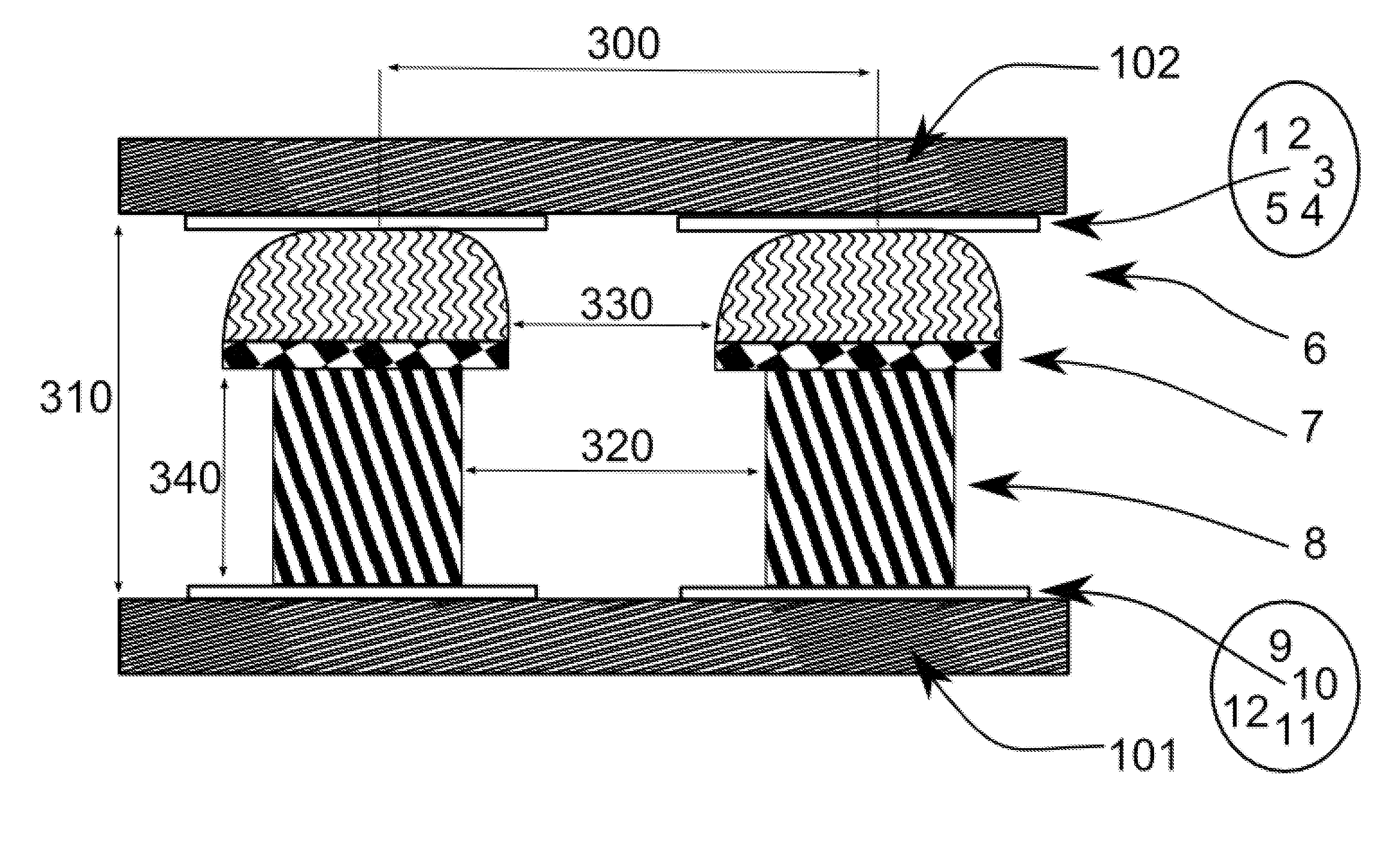
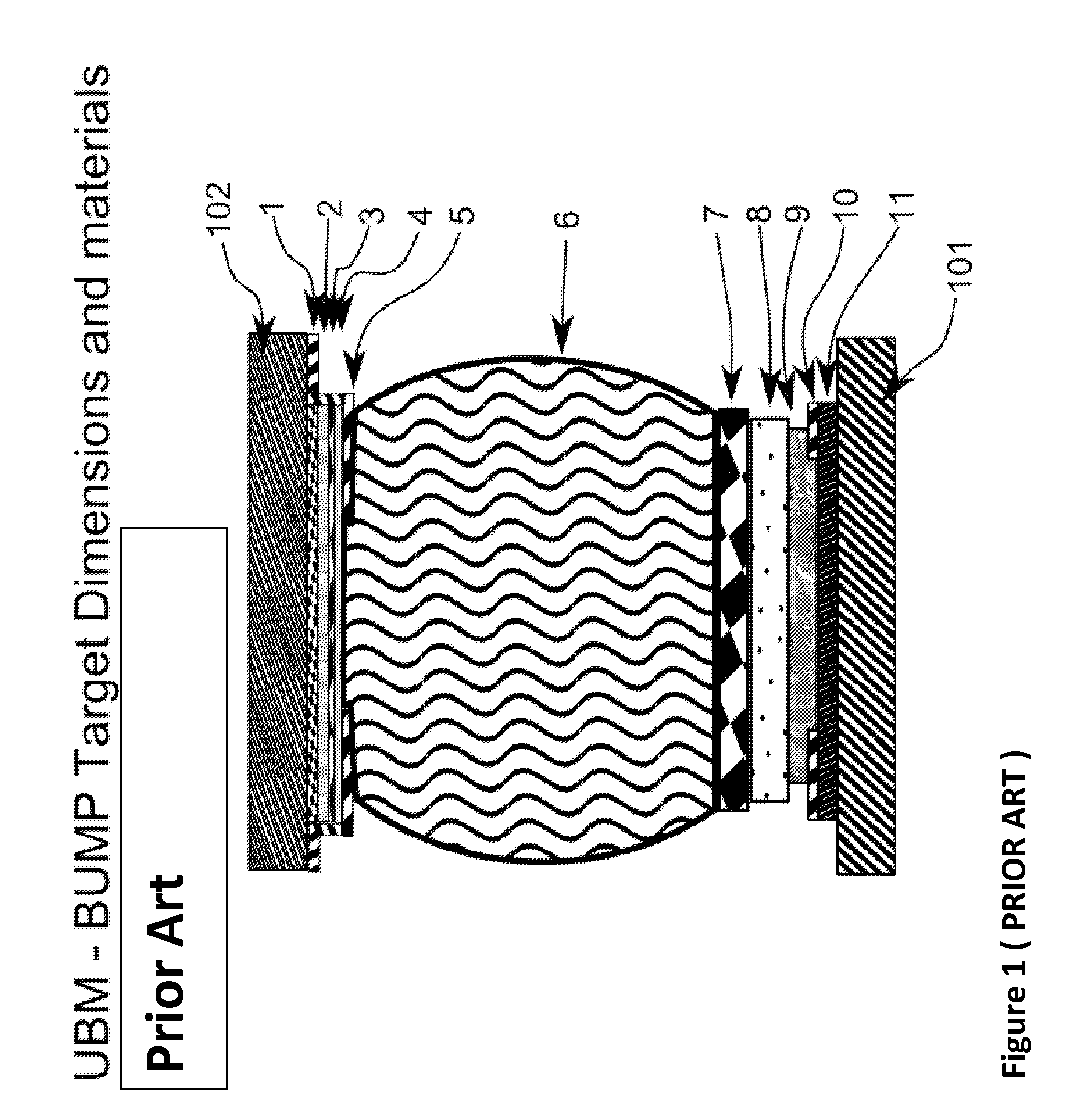
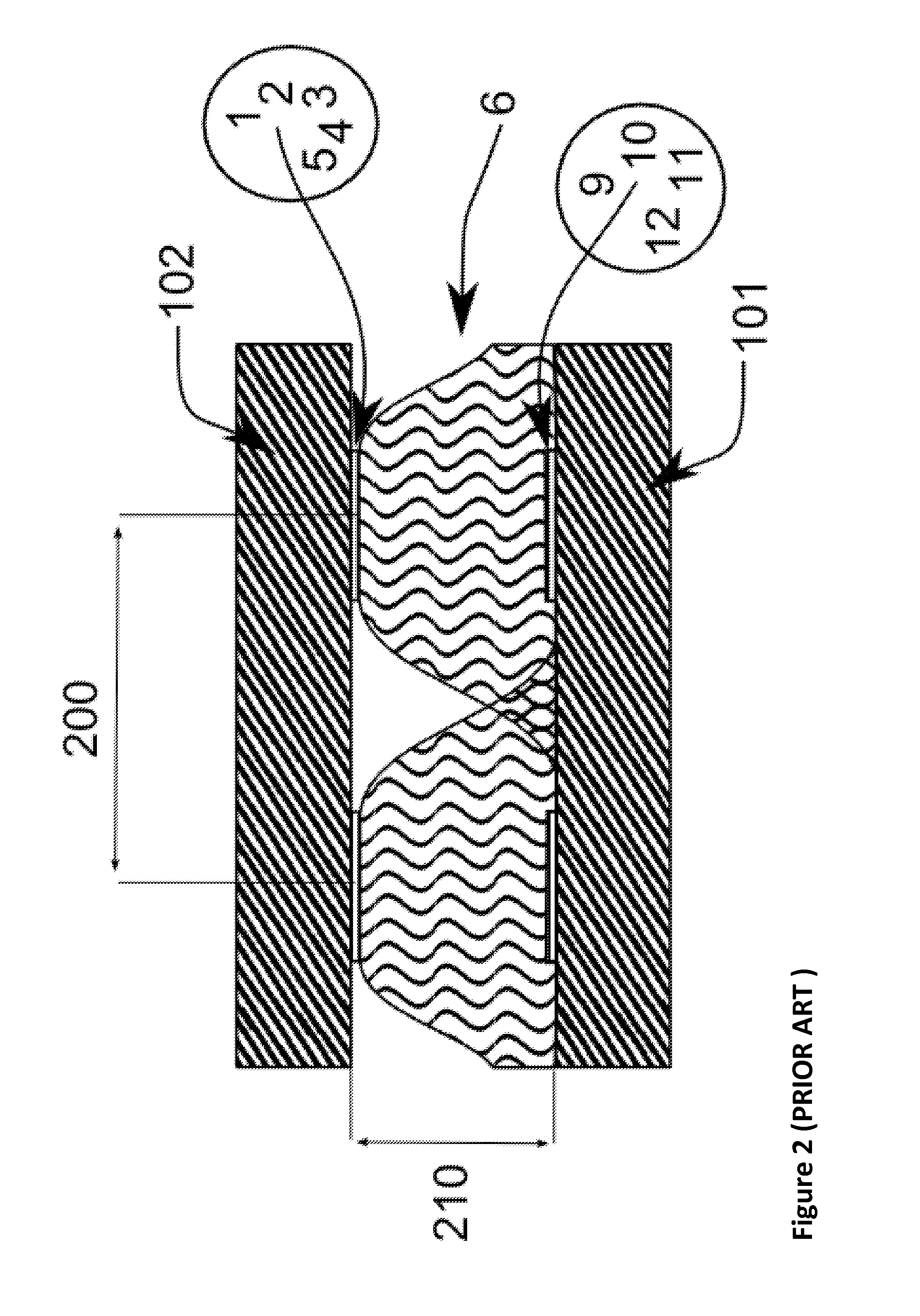
[0019]With reference to FIG. 1, an imaging device in accordance with prior art is shown where a CMOS pixel 101 is bump-bonded to the corresponding detector pixel 102 via bump 6. A bump 6 of the prior art is seen on a semiconductor readout pixel 101 (e.g., a CMOS). The bump 6 is of spherical shape. Under the bump one or more seed metal layers have been deposited. Typically, the seed layers are grown on the CMOS readout wafer 101 via sputtering or evaporation technique. The bump-bonded imaging device of the prior art is shown in FIG. 1 and Table 1 all the elements are described with like numbers in the table below, indicating also the average thickness:

TABLE 1Thickness (um) (exampleNameNumberMaterialaverage)Detector pad1Pt (Platinum)0.050UBM 12Au (Gold)0.030UBM 23Ni (Nickel)0.050UBM 34Au (Gold)0.080Detector passivation5AlN0.150(AluminumNitride)Bump solder6SnBi10.000(Tin Bismuth)Bump pedestal7Ni (Nickel)1.600Bump seed bulk8Cu (Copper)0.500Bump seed adhesion9TiW (Titanium0.040tangsten)C...


PUM


Abstract

A high pixel density intraoral x-ray imaging sensor includes a direct conversion, fully depleted silicon detector bump bonded to a readout CMOS substrate by capillary bump bonds.

Description

BACKGROUND OF THE INVENTION[0001]The current invention relates to a direct conversion, semiconductor x-ray imaging device where the detector substrate is bump bonded to the readout substrate. X-rays (or other type of radiation) impinge upon the detector and electron-holes pairs are created inside the detector substrate (thus the term “direct conversion”) in response to the absorbed energy. Under the influence of an electric field applied across the detector these electron(holes) are transferred to charge collection electrodes. The charge collection electrodes are connected to corresponding readout electrodes on a readout substrate, which act as the input to a readout pixel on the readout substrate. The connection is made via bumps and the known flip-chip bonding technique.DESCRIPTION OF THE RELATED ART[0002]The technique of bumping and flip-chip bonding is wide spread in the manufacturing of direct conversion x-ray imaging devices. Typically the bumps are grown with electroplating o...

Claims


Application Information

Patent Timeline
IPC IPC(8): G01T1/24
CPCG01T1/247H01L27/14661A61B6/145H01L28/00H01L27/14634H01L27/14659H01L27/14636H01L2224/13017H01L27/14658H01L31/028
Inventor SPARTIOTIS, KONSTANTINOSNYKANEN, HENRI TAPIOLIN, LIMINLAHTINEN, TUOMAS HEIKKI ELMERILAUKKA, PASI JUHANI
Owner OY AJAT LTD
Why Eureka
Try Eureka