Sub-band infra-red irradiation for detector crystals

a detector crystal and sub-band technology, applied in the field of radiation detectors, can solve the problems of insufficient or even no charge collection, and insufficient radiation detection speed, and achieve the effect of less polarization and more efficient radiation detection

Active Publication Date: 2015-10-08
KONINKLJIJKE PHILIPS NV
View PDF7 Cites 2 Cited by
  • Summary
  • Abstract
  • Description
  • Claims
  • Application Information

AI Technical Summary

Benefits of technology

[0006]It is an object of the present invention to provide more efficient radiation detection with less polarization in the conversion material.

Problems solved by technology

For future garnet based scintillators this may change, however, for such devices also very fast photodiodes are needed, which have to convert the light into electrical signals.
However, CZT material is prone to polarization, i.e. formation of a space-charge within a pixel volume when irradiated with X-rays, which space-charge weakens the applied electrical field so that electron-hole pairs, which are generated in an interaction of an X-ray photon with the CZT material, no longer drift fast enough towards the anode and cathode.
As a consequence, insufficient or even no charge is collected, and the measurement result is simply wrong.

Method used


Image

  • Sub-band infra-red irradiation for detector crystals
  • Sub-band infra-red irradiation for detector crystals
  • Sub-band infra-red irradiation for detector crystals

Examples


first embodiment

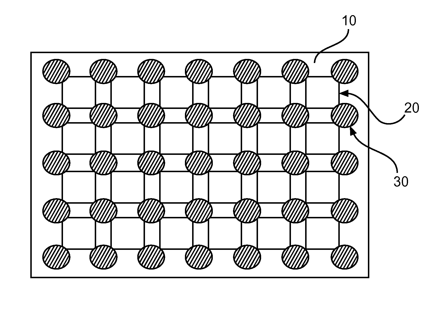
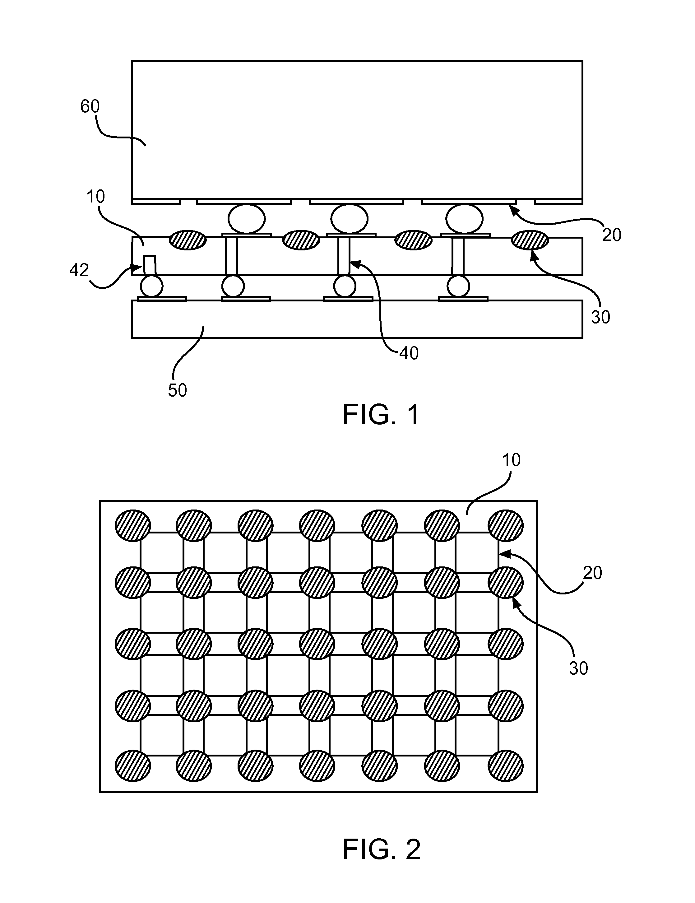
[0028]FIG. 1 shows schematically and exemplarily a cross-sectional side view of a radiation detector with an IR LED layer 10 interposed between a 4-side-buttable CMOS (Complementary Metal Oxide Semiconductor) readout circuit or chip 50, e.g. and application specific integrated circuit (ASIC), and a CZT crystal 60. The CZT crystal 60 is flip-chip bonded via pixel pads 20 to a substrate (i.e. IR LED layer 10 and readout chip 50) which does the readout. More specifically, an IR irradiation device (i.e. the IR LED layer 10) is integrated into the readout chip 50 to which the CZT crystal 60 is flip-chip bonded, so that a 4-side-buttable crystal is achieved, in which electrical input / output circuits are arranged under the device rather than at its edge. This 3-D packaging allows extremely close spacing of radiation detectors.

[0029]Irradiation with sub-band IR LED light, where the optical photons have an energy which is smaller than the band gap, reduces the tendency towards polarization ...

second embodiment

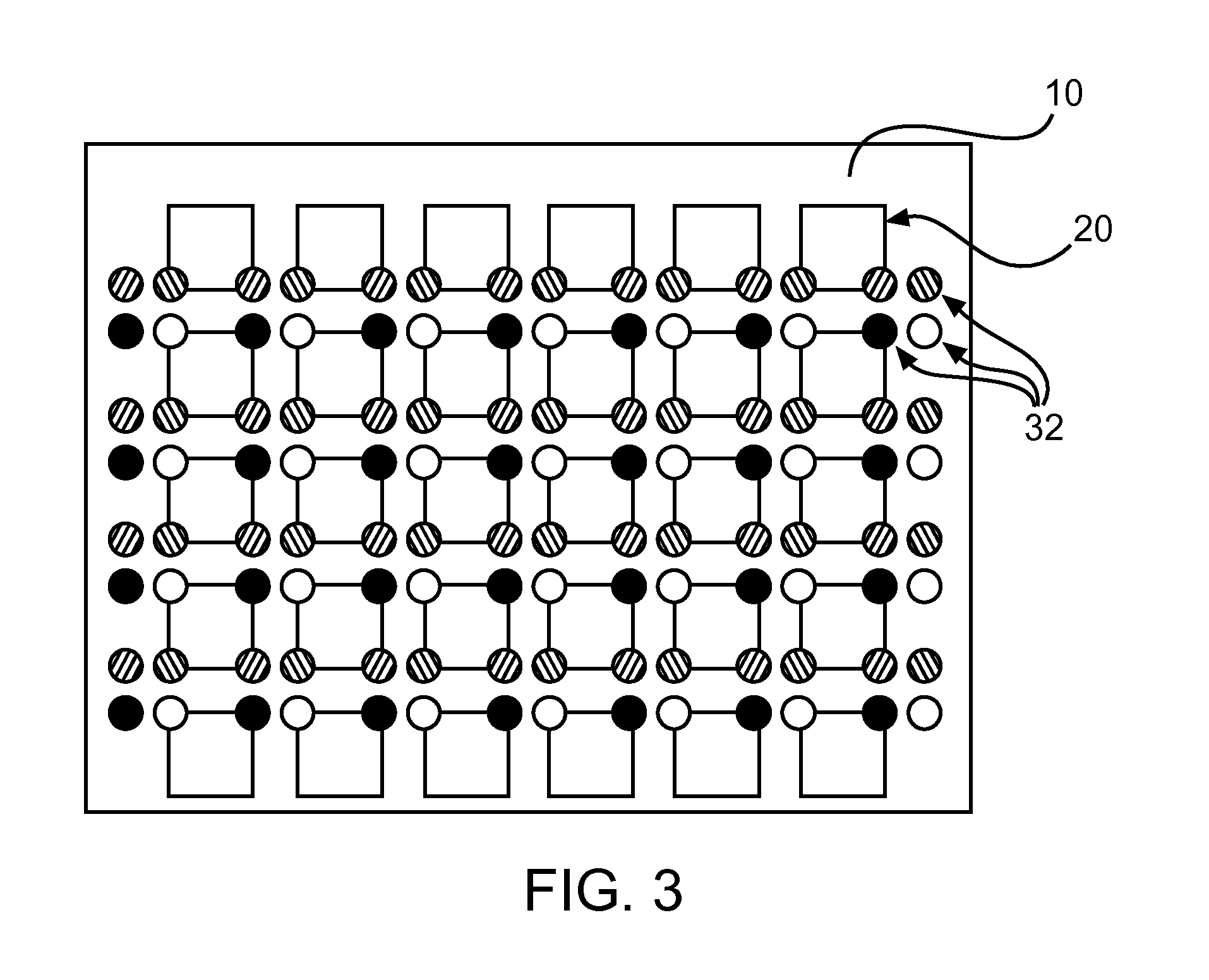
[0030]Hence, as indicated in FIG. 1, the pixels of the readout electronics of the readout chip 50 are bonded via respective solder bumps and through connection portions 40 directly to the pixel pads 20 of the CZT crystal 60. Additionally, a supply contact 42 for the IR LED layer 10 is provided. The substrate with the readout circuit also implements—besides the readout electronics—one or more sub-band IR LED sources 30. Optionally, as described below in connection with the second embodiment, more than one IR LED source 30 per pixel may be implemented, if different IR light wavelengths are to be used, which may help to release even more charges of deep traps of different energies.

[0031]Alternatively, it may suffice to implement the IR LED sources 30 only in a sub-set of pixels. Since the IR LED sources 30 may be manufactured from GaAs or AlGaAs material which differs from CMOS, the IR LED sources 30 can be implemented on a different substrate (i.e. the IR LED layer 10), which is then ...


PUM


Abstract

The invention relates to radiation detection with a directly converting semiconductor layer for converting an incident radiation into electrical signals. Sub-band infra-red (IR) irradiation considerably reduces polarization in the directly converting semi-conductor material when irradiated, so that counting is possible at higher tube currents without any baseline shift. An IR irradiation device is integrated into the readout circuit to which the crystal is flip-chip bonded in order to enable 4-side-buttable crystals.

Description

FIELD OF THE INVENTION[0001]The invention relates to the field of radiation detectors such as—but not limited to—X-ray detectors comprising a directly converting semiconductor layer for converting an incident radiation into electrical signals. More specifically, the invention relates to the field of photon-counting (energy resolving) detectors e.g. for human medical imaging or other purposes.BACKGROUND OF THE INVENTION[0002]X-ray detectors comprising a directly converting semiconductor layer enable individual X-ray quanta or photons to be detected quantitatively and energy-selectively. In the case of this type of X-ray detectors, an incident X-ray photon generates free charge carriers in the form of electron-hole pairs in the semiconductor layer on account of in part multistage physical interaction processes with a semiconductor material. By way of example, semiconductor materials in the form of CdTe, CdZnTe (CZT), CdTeSe, CdZnTeSe, CdMnTe, InP, TIBr2 or HGI2 are suitable for detect...

Claims


Application Information

Patent Timeline
Patent Type & Authority Applications(United States)
IPC IPC(8): G01J1/44H01L31/09H01L31/0296H01L31/08G01T1/00H01L31/18
CPCG01J1/44G01T1/00H01L31/1832G01J2001/4446H01L31/085H01L31/09H01L31/02966G01T1/24
Inventor HERRMANN, CHRISTOPHSTEADMAN BOOKER, ROGER
Owner KONINKLJIJKE PHILIPS NV
Why Eureka
Try Eureka