Epitaxial wafer and a method of manufacturing thereof

a technology of epitaxial wafers and manufacturing methods, applied in the direction of basic electric elements, electrical apparatus, semiconductor devices, etc., can solve the problems of damage or even destruction of electronic device structures, detrimental to the functional integrity of electronic devices, etc., to reduce the nucleation and propagation of dislocations, the effect of less complex and more effectiv

Active Publication Date: 2015-10-22
SILTRONIC AG +1
View PDF3 Cites 8 Cited by
  • Summary
  • Abstract
  • Description
  • Claims
  • Application Information

AI Technical Summary

Benefits of technology

[0010]An object of the present invention is to provide a solution to the above mentioned problems which is less complex and more effective than known solutions. The inventors have found that the presence of nitrogen in the silicon epitaxial layer at a concentration of 1×10¹⁶ atoms / cm3 or more and 1×10²⁰ atoms / cm3 or less reduces the nucleation and propagation of dislocations. Moreover, nitrogen incorporated into the silicon epitaxial layer in accordance with the present invention is readily accessible for oxygen-nitrogen interaction, which allows the formation of an oxygen-enriched region having an oxygen peak-concentration in a certain depth from the surface of the epitaxial layer. The oxygen-enriched region exhibits gettering activity for metallic impurities.

Problems solved by technology

Miniaturization of electronic device structures like transistors is in progress and amplifies several problems.
It becomes more likely that dislocations caused by stress fields will damage or even destroy electronic device structures.
Another problem concerns metallic impurities which have a detrimental effect on the functional integrity of electronic devices.

Method used


Image

  • Epitaxial wafer and a method of manufacturing thereof
  • Epitaxial wafer and a method of manufacturing thereof
  • Epitaxial wafer and a method of manufacturing thereof

Examples


example

Getter Test

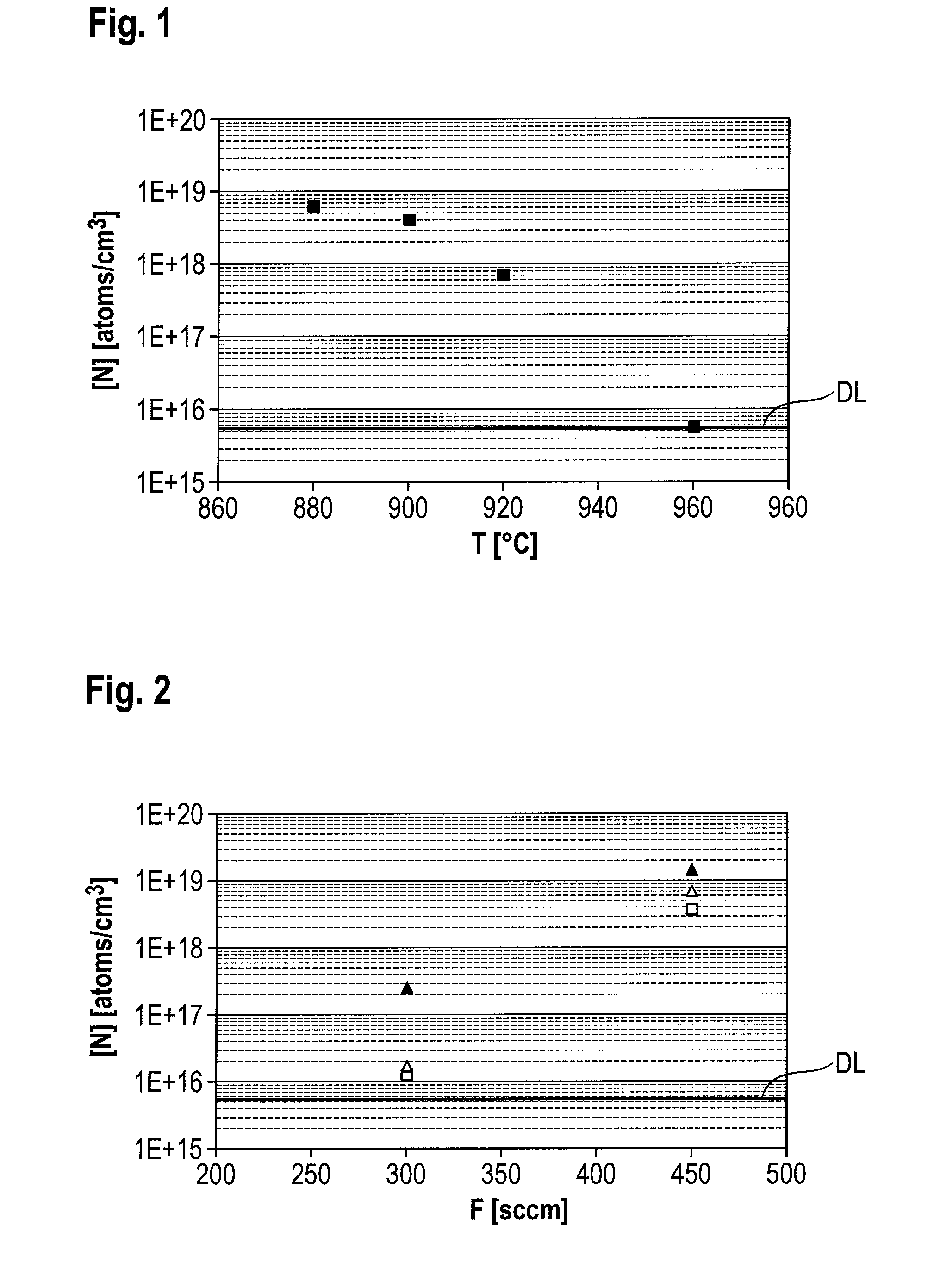
[0064]Two different samples of epitaxial wafers were prepared, sample 4 representing the present invention and sample 5 representing a comparative example.

[0065]The epitaxial wafers according to sample 4 were prepared by depositing a silicon epitaxial layer on the polished front side of a silicon substrate wafer by chemical vapor deposition in the presence of a deposition gas atmosphere containing dichlorosilane as silicon precursor compound and ammonia as nitrogen precursor compound. The deposition temperature was set to 880° C. The silicon substrate wafer had a resistivity of 60 Ωcm and an oxygen concentration of 5×10¹⁷ atoms / cm3 (new ASTM).

[0066]The epitaxial wafers according to sample 5 were prepared in the same manner, except that the deposition gas did not contain a nitrogen precursor compound, i.e. the silicon epitaxial layer was not doped with nitrogen.

[0067]The back side of each sample wafer was contaminated with a Ni-containing salt by spin coating. The Ni conta...


PUM

PropertyMeasurementUnit
temperatureaaaaaaaaaa
resistivityaaaaaaaaaa
concentrationaaaaaaaaaa

Abstract

An epitaxial wafer comprises a silicon substrate wafer having first and second sides, and a silicon epitaxial layer deposited on the first side, and optionally one or more additional epitaxial layers on top of the silicon epitaxial layer, at least one of the silicon epitaxial layer or at least one of the one or more additional epitaxial layers being doped with nitrogen at a concentration of 1×10¹⁶ atoms/cm3 or more and 1×10²⁰ atoms/cm3 or less. The epitaxial wafer is produced by depositing the silicon epitaxial layer and/or at least one of the one or more additional epitaxial layers, at a deposition temperature of 940° C. or less through chemical vapor deposition in the presence of a deposition gas atmosphere containing one or more silicon precursor compounds and one or more nitrogen precursor compounds.

Description

CROSS REFERENCE TO RELATED APPLICATIONS[0001]This application is the U.S. National Phase of PCT Appln. No. PCT / EP2013 / 075313 filed Dec. 3, 2013, which claims the benefit of 61 / 733,977 filed Dec. 6, 2012, the disclosures of which are incorporated in their entirety by reference herein.BACKGROUND OF THE INVENTION[0002]1. Field of the Invention[0003]The claimed invention is directed to an epitaxial wafer and to a method for producing the epitaxial wafer.[0004]2. Description of the Related Art[0005]Epitaxial wafers comprise a silicon substrate wafer having a first side and a second side, and a silicon epitaxial layer deposited on the first side of the silicon substrate wafer. Such wafers are prepared by depositing the silicon epitaxial layer on the first side of the silicon substrate wafer by chemical vapor deposition (CVD). Epitaxial wafers are used for manufacturing semiconductor devices such as memory devices and microprocessors.[0006]Miniaturization of electronic device structures li...

Claims


Application Information

Patent Timeline
Patent Type & Authority Applications(United States)
IPC IPC(8): H01L21/322H01L29/167H01L21/02
CPCH01L21/3225H01L21/0257H01L29/167H01L21/0262H01L21/0254H01L21/02381H01L21/02532H01L21/02573H01L21/3221
Inventor STORCK, PETERWERNER, NORBERTVORDERWESTNER, MARTINTOLCHINSKY, PETERYABLOK, IRWIN
Owner SILTRONIC AG
Why Eureka
Try Eureka