Nitride semiconductor device

Active Publication Date: 2015-10-22
PANASONIC INTELLECTUAL PROPERTY MANAGEMENT CO LTD
View PDF4 Cites 5 Cited by
  • Summary
  • Abstract
  • Description
  • Claims
  • Application Information

AI Technical Summary

Benefits of technology

[0024]This structure provides a nitride semiconductor transistor having the foregoing characteristics. More specifically, this structure provides a nitride semiconductor transistor capable of reducing both on

Problems solved by technology

However, a Schottky diode has a disadva

Method used


Image

  • Nitride semiconductor device
  • Nitride semiconductor device
  • Nitride semiconductor device

Examples


first exemplary embodiment

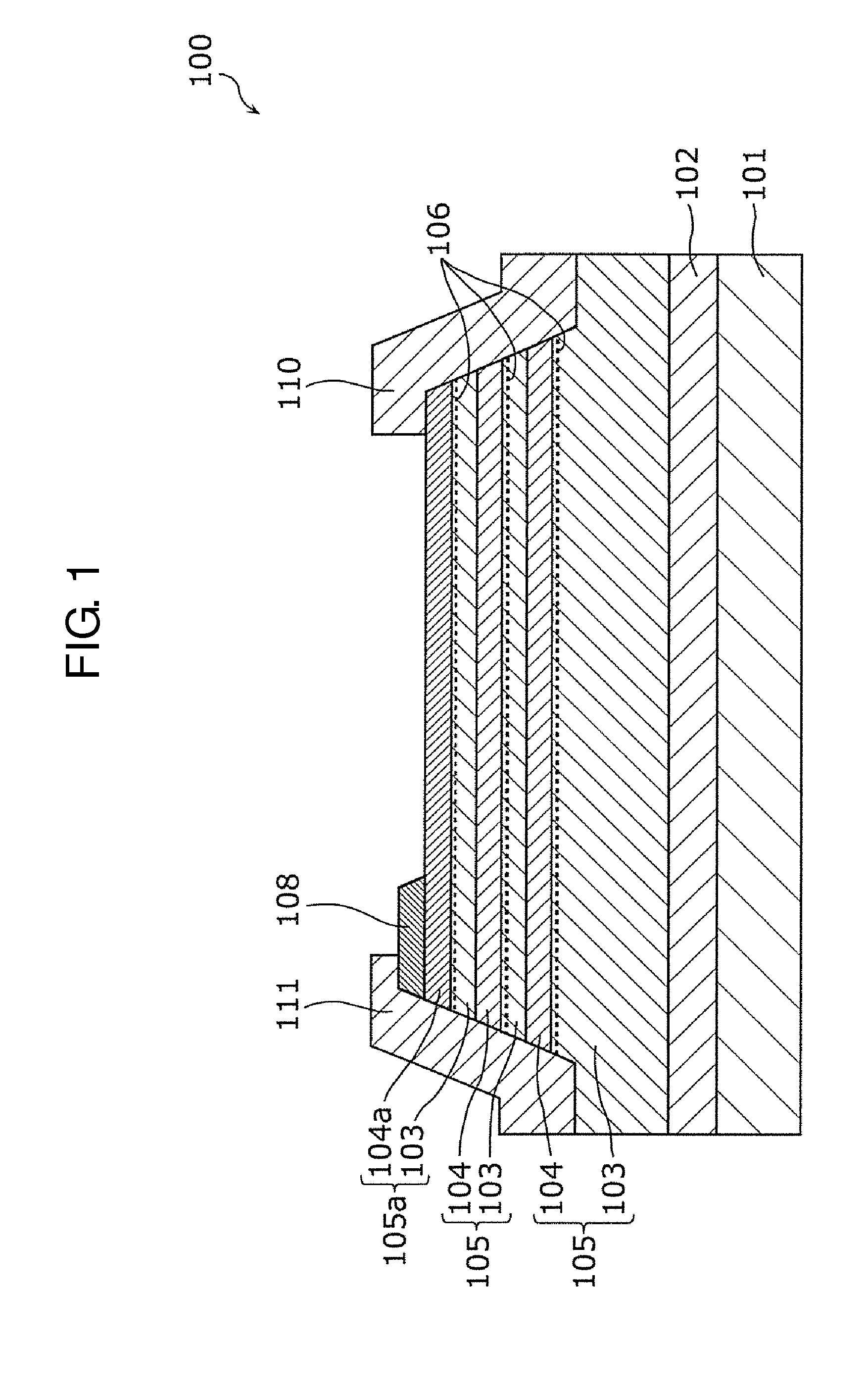
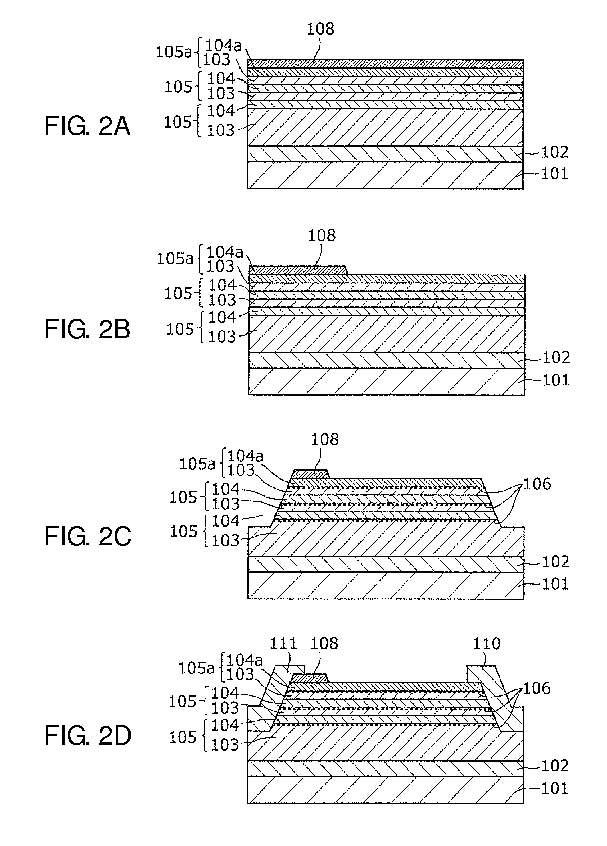
[0045]FIG. 1 is a cross-sectional view illustrating a configuration of a nitride semiconductor device according to a first exemplary embodiment. A diode is herein discussed as an example of the nitride semiconductor device in this exemplary embodiment.

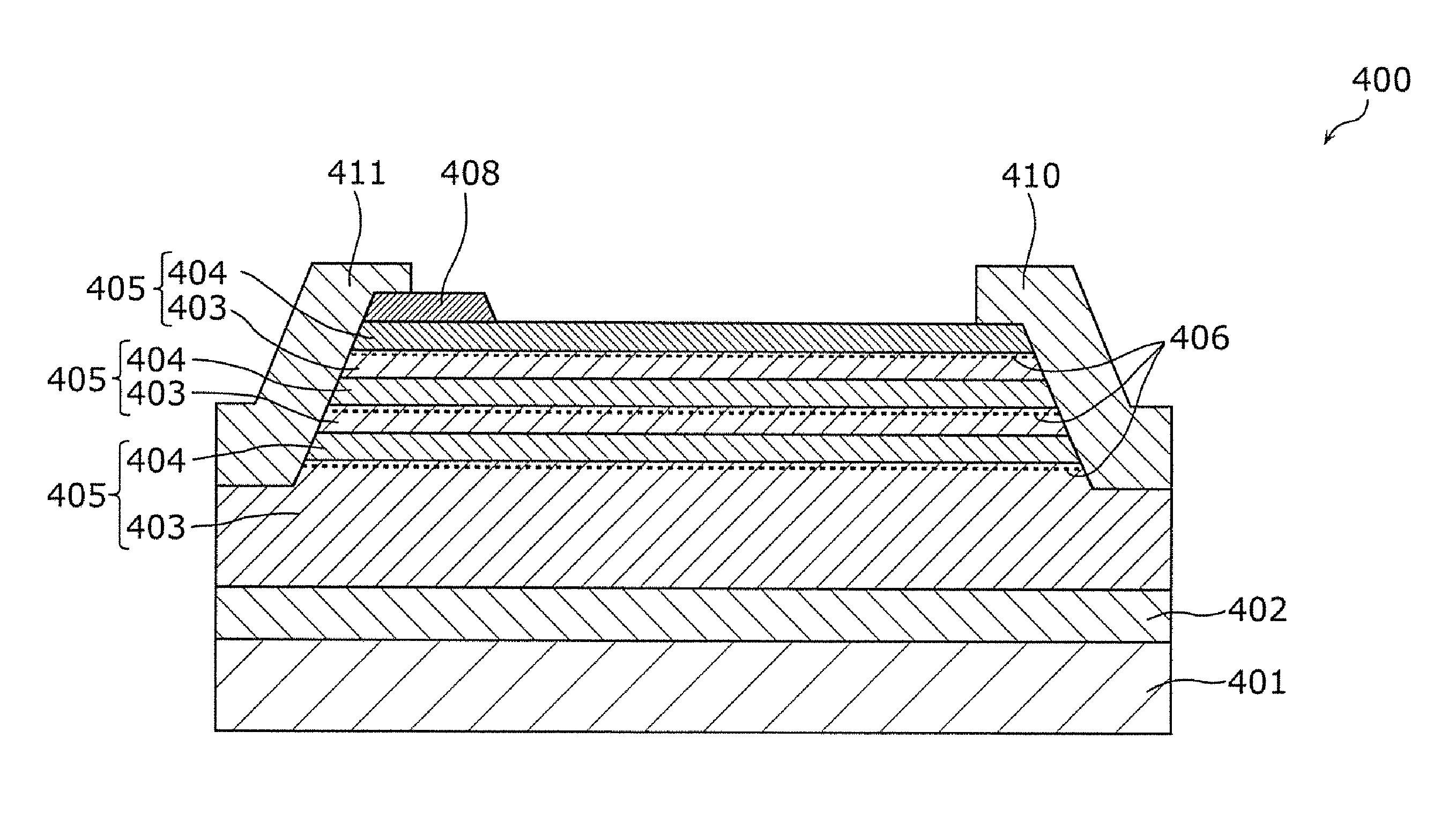
[0046]Diode 100 of this exemplary embodiment includes substrate 101, buffer layer 102, semiconductor layers 105 each constituted by undoped GaN layer 103 and undoped AlGaN layer 104, block layer 108 formed on undoped AlGaN layer 104a which is an uppermost layer of three laminated layers of semiconductor layers 105, cathode electrode 110, anode electrode 111.

[0047]More specifically, as illustrated in FIG. 1, diode 100 includes buffer layer 102 having a film thickness of 2 μm, undoped GaN layer 103 having a film thickness of 3 μm, and undoped AlGaN layer 104 having a film thickness of 25 nm in this order on substrate 101 constituted by Si, sapphire, SiC, GaN, or others. Laminated on undoped GaN layer 104 is semiconductor layer 105 consti...

first embodiment

Modification of First Embodiment

[0067]A modification according to the first exemplary embodiment is hereinafter described. A diode corresponding to a nitride semiconductor device according to this modification is different from diode 100 according to the first exemplary embodiment in that a film thickness of uppermost undoped AlGaN layer 104a is larger than each film thickness of other undoped AlGaN layers 104. Constituent elements in this modification similar to the corresponding constituent elements in the first exemplary embodiment have been given similar reference numbers.

[0068]FIGS. 5 and 6 are cross-sectional views illustrating configurations of diodes 150 and 180, respectively, according to this modification.

[0069]As illustrated in FIG. 5, uppermost undoped AlGaN layer 104b provided immediately below the p-AlGaN layer constituting block layer 108 has a large film thickness. The channel immediately below p-AlGaN layer has higher resistance in a state of forward bias in accorda...

second exemplary embodiment

Modification of Second Exemplary Embodiment

[0085]A modification of the second exemplary embodiment is hereinafter described. A transistor corresponding to a nitride semiconductor device according to this modification is different from transistor 200 according to the second exemplary embodiment in that a gate recess is formed below a gate electrode.

[0086]FIG. 9 is a cross-sectional view illustrating a configuration of the transistor according to this modification.

[0087]As illustrated in FIG. 9, block layer 312 of transistor 300 is configured to cover a recess region (gate recess) etched in such a shape as to penetrate semiconductor layer 205 constituted by undoped AlGaN layer 204 and undoped GaN layer 203. This structure allows easier control over a threshold of transistor 300 in comparison with a structure including no gate recess.

[0088]More specifically, in manufacturing normally-off operation type transistor 300, for example, a gate recess to be formed is configured to reach a low...


PUM


Abstract

A nitride semiconductor device includes: a substrate; a buffer layer formed on the substrate; a laminated body formed by two or more cycles of semiconductor layers each including a first nitride semiconductor layer, and a second nitride semiconductor layer having a larger band gap than a band gap of the first nitride semiconductor layer, the first and second nitride semiconductor layers being laminated in this order on the buffer layer; a first electrode; and a second electrode. A channel layer is formed in each of the semiconductor layers at an interface between the first nitride semiconductor layer and the second nitride semiconductor layer. A carrier concentration of the channel layer in the uppermost semiconductor layer is lower than a carrier concentration of each of the channel layers of the other semiconductor layers.

Description

BACKGROUND OF THE INVENTION[0001]1. Field of the Invention[0002]The present disclosure relates to a nitride semiconductor device applicable to a power device included in a power supply circuit of a television set or other consumer products.[0003]2. Description of the Related Art[0004]A nitride semiconductor, including a GaN semiconductor as a typical example, has a wide gap. For example, GaN and AlN semiconductors have wide band gaps of 3.4 eV and 6.2 eV at room temperature, respectively. Accordingly, a nitride semiconductor is characterized by a higher breakdown electric field, and a higher saturated electron drift velocity than that velocity of a compound semiconductor such as a GaAs semiconductor or of a Si semiconductor. In AlGaN / GaN heterostructure, charges are generated at a heterointerface as a result of spontaneous polarization and piezoelectric polarization on (0001) plane. In this case, a sheet carrier concentration of 1×1013 cm−2 or higher is obtained even in an undoped s...

Claims


Application Information

Patent Timeline
IPC IPC(8): H01L29/778H01L29/20H01L29/06H01L29/205H01L29/10H01L29/872
CPCH01L29/7787H01L29/1033H01L29/2003H01L29/0684H01L29/205H01L29/872H01L29/42316H01L29/66462H01L29/1029H01L29/66212H01L29/41766H01L29/7783H01L29/1066
Inventor SHIBATA, DAISUKENEGORO, NOBORU
Owner PANASONIC INTELLECTUAL PROPERTY MANAGEMENT CO LTD
Why Eureka
Try Eureka