Novel semiconductor device and structure

a semiconductor and integrated circuit technology, applied in the field of integrated circuit devices and fabrication methods, can solve the problems of many barriers to practical implementation of 3d stack chips, difficult integration of memory such as dram with logic technologies, and increase the cost of adding additional costs, so as to achieve the effect of improving speed, small footprint, and improving performan

Active Publication Date: 2015-11-26
MONOLITHIC 3D
View PDF42 Cites 49 Cited by
  • Summary
  • Abstract
  • Description
  • Claims
  • Application Information

AI Technical Summary

Benefits of technology

[0018]The 3D ICs offer many significant potential benefits, including a small footprint—more functionality fits into a small space. This extends Moore's Law and enables a new generation of tiny but powerful devices. The 3D ICs have improved speed—The average wire length becomes much shorter. Because propagation delay may be proportional to the square of the wire length, overall performance increases. The 3D ICs consume low power—Keeping a signal on-chip reduces its power consumption by ten to a hundred times. Shorter wires also reduce power consumption by producing less parasitic capacitance. Reducing the power budget leads to less heat generation, extended battery life, and lower cost of operation. The vertical dimension adds a higher order of connectivity and opens a world of new design possibilities. Partitioning a large chip to be multiple smaller dies with 3D stacking could potentially improve the yield and reduce the fabrication cost. Heterogeneous integration—Circuit layers can be built with different processes, or even on different types of wafers. This means that components can be optimized to a much greater degree than if built together on a single wafer. Components with incompatible manufacturing could be combined in a single device. The stacked structure may hinder attempts to reverse engineer the circuitry. Sensitive circuits may also be divided among the layers in such a way as to obscure the function of each layer. 3D integration may allow large numbers of vertical vias between the layers. This may allow construction of wide bandwidth buses between functional blocks in different layers. A typical example would be a processor and memory 3D stack, with the cache memory stacked on top of the processor. This arrangement may allow a bus much wider than the typical 128 or 256 bits between the cache and processor. Wide buses in turn alleviate the memory wall problem.

Problems solved by technology

Additionally, integrating memories such as DRAM with logic technologies may be difficult, and may add additional costs.
However, there may be many barriers to practical implementation of 3D stacked chips.
Copper or Aluminum wiring levels, in fact, can get damaged when exposed to temperatures higher than about 400° C. If transistors were arranged in 3 dimensions along with wires, it may have the challenge described below.
When the Top Transistor Layer is constructed using Temperatures higher than about 700° C., it can damage the Bottom Wiring Layer.Generally due to the above mentioned problem with forming transistor layers above wiring layers at temperatures lower than about 400° C., the semiconductor industry has largely explored alternative architectures for 3D stacking.
Unfortunately, the size of Contacts to the other Layer may be large and the number of these Contacts may be small.
This low connectivity between layers may be because of two reasons: (i) Landing pad size may need to be relatively large due to alignment issues during wafer bonding.
This misalignment between two wafers may potentially limit the minimum contact landing pad area for electrical connection between two layers; (ii) The contact size may need to be relatively large.
Etching deep holes in silicon with small lateral dimensions and filling them with dielectric and metal to form TSVs may not be easy.
Therefore, connectivity between two the embedded memory and logic transistors may be limited.
Unfortunately, however, almost all semiconductor devices in the market today (logic, DRAM, flash memory) utilize horizontal (or planar) transistors due to their many advantages, and it may be difficult to convince the industry to move to vertical transistor technology.
The stacked structure may hinder attempts to reverse engineer the circuitry.

Method used


Image

  • Novel semiconductor device and structure
  • Novel semiconductor device and structure
  • Novel semiconductor device and structure

Examples


Embodiment Construction

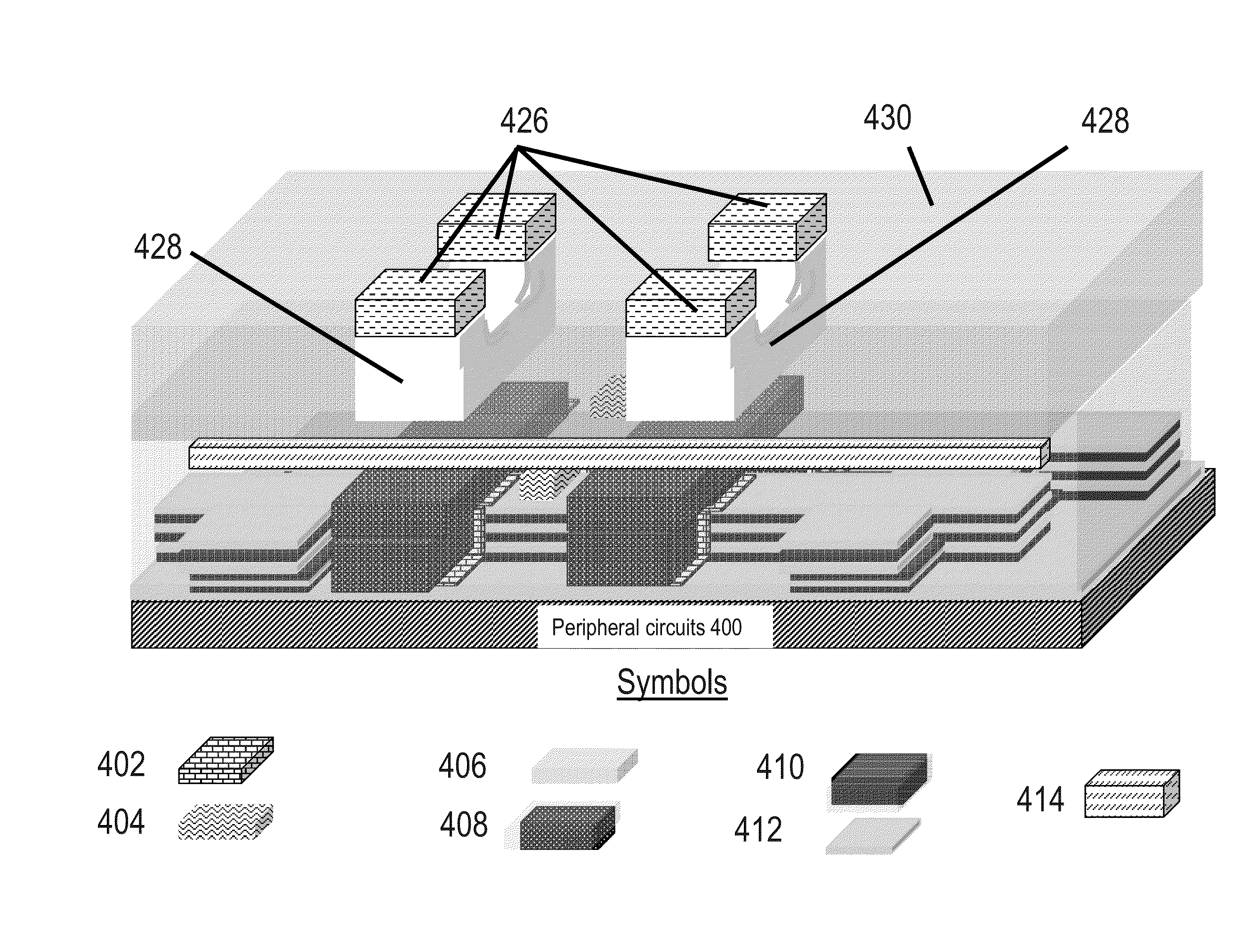
[0064]Embodiments of the invention are described herein with reference to the drawing figures. Persons of ordinary skill in the art will appreciate that the description and figures illustrate rather than limit the invention and that in general the figures are not drawn to scale for clarity of presentation. Such skilled persons will also realize that many more embodiments are possible by applying the inventive principles contained herein and that such embodiments fall within the scope of the invention which is not to be limited except by the appended claims.

[0065]Some drawing illustration figures may describe process flows for building devices. These process flows, which may be a sequence of steps for building a device, may have many structures, numerals and labels that may be common between two or more adjacent steps. In such cases, some labels, numerals and structures used for a certain step's figure may have been described in the previous steps' figures.

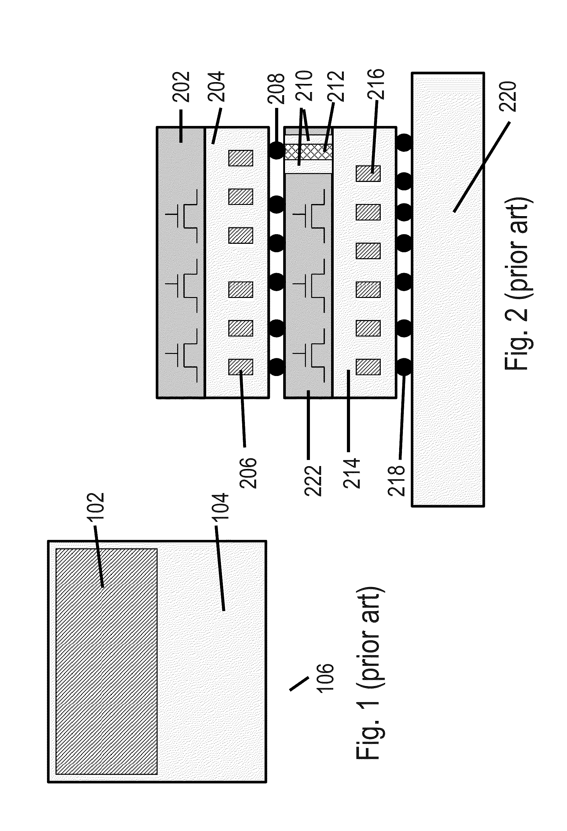
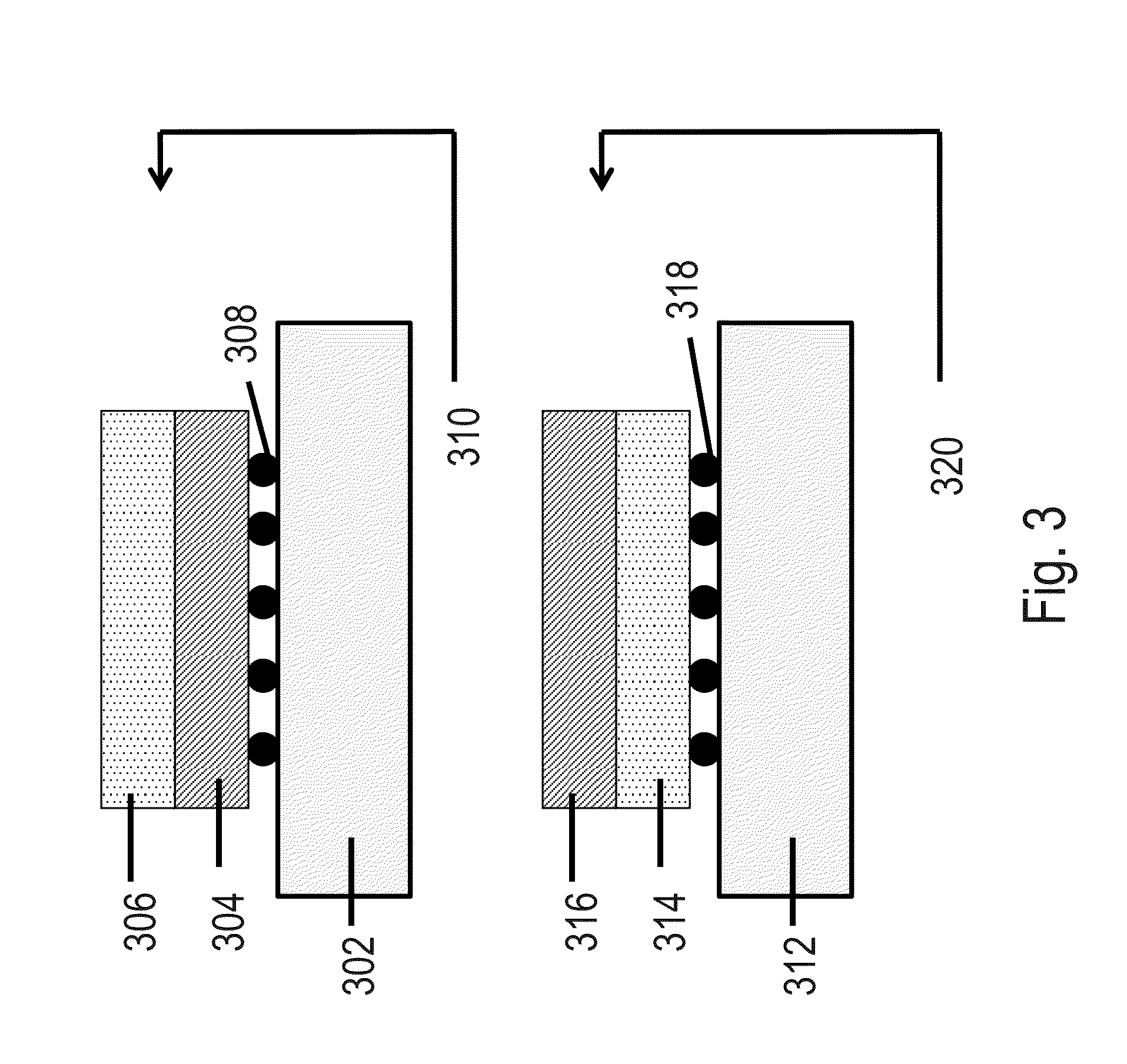
[0066]FIG. 1 illustrates an...


PUM


Abstract

A 3D device, including: a first layer including a first memory including a first transistor; and a second layer including a second memory including a second transistor; where the second transistor is self-aligned to the first transistor, and where the first transistor and the second transistor each being a junction-less transistor.

Description

BACKGROUND OF THE INVENTION[0001]1. Field of the Invention[0002]This application relates to the general field of Integrated Circuit (IC) devices and fabrication methods, and more particularly to multilayer or Three Dimensional Integrated Circuit (3D IC) devices and fabrication methods.[0003]2. Discussion of Background Art[0004]Logic chips such as microprocessors and Systems-on-Chips (SoCs) typically include a significant amount of on-die memory. This on-die memory can be in the form of Static Random Access Memory (SRAM), Dynamic Random Access Memory (DRAM), Flash Memory and / or another type of memory. In many chips today, as much as 50%-80% of the die area could be consumed by these memory types. Additionally, integrating memories such as DRAM with logic technologies may be difficult, and may add additional costs. Techniques to reduce area overhead of memories embedded on the chip, henceforth referred to as embedded memory, will be useful. Methods to improve performance of embedded m...

Claims


Application Information

Patent Timeline
Patent Type & Authority Applications(United States)
IPC IPC(8): H01L23/528H01L27/108H01L27/115H01L27/24
CPCH01L23/528H01L27/2436H01L27/10805H01L27/1157H01L27/11526H01L27/11573H01L27/11524H01L27/10897G11C8/16H01L27/0688H01L2224/16145H01L2224/32145G11C13/0007G11C2213/71G11C2213/75G11C5/025G11C5/04G11C11/403H10B63/30H10B63/84H10N70/20H10N70/823H10N70/883H10N70/8833H10B12/20H10B12/30H10B63/845H10N70/24H10N70/231H10N70/245H10N70/882H10N70/8836
Inventor OR-BACH, ZVICRONQUIST, BRIAN
Owner MONOLITHIC 3D
Why Eureka
Try Eureka