
Device Isolation for III-V Substrates

a technology of iiiv semiconductor and device isolation, which is applied in the direction of semiconductor devices, basic electric elements, electrical apparatus, etc., can solve the problems of strain in the sige layer, increased strain, and difficulty in lattice mismatch,

Inactive Publication Date: 2015-12-10
ELPIS TECH INC
View PDF1 Cites 11 Cited by
  • Summary
  • Abstract
  • Description
  • Claims
  • Application Information

AI Technical Summary

Benefits of technology

This patent text describes methods for making semiconductor devices using III-V materials on a substrate. The process includes forming layers of iron-doped indium phosphide and epitaxial III-V semiconductor material, and then patterning the semiconductor material to create active areas of the device. The technical effect is the improved isolation of devices on III-V semiconductor substrates, which allows for more complex circuit design and better performance of the resulting devices.

Problems solved by technology

However, this will cause strain in the SiGe layer, and that strain will increase as more SiGe is grown.
For the above-described reasons, the lattice mismatch problem remains a challenge for implementing III-V semiconductor materials in device fabrication that uses heterogeneous epitaxial layers or substrate (e.g., forming III-V epitaxial layers on a silicon substrate).
However, unlike silicon-on-insulator (SOI) substrates where device isolation is easily achieved by etching the SOI layer which rests on a buried oxide (or BOX), III-V devices that are made on virtual III-V on silicon substrates do not have a convenient way of achieving isolation.

Method used


Image

  • Device Isolation for III-V Substrates
  • Device Isolation for III-V Substrates
  • Device Isolation for III-V Substrates

Examples


Embodiment Construction

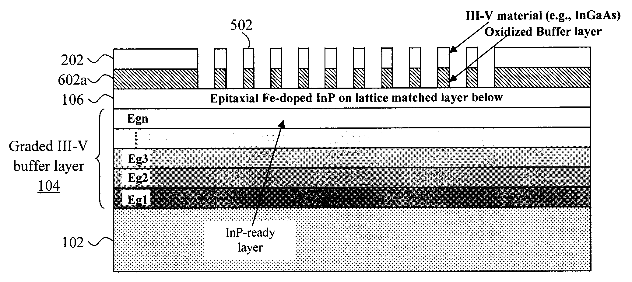
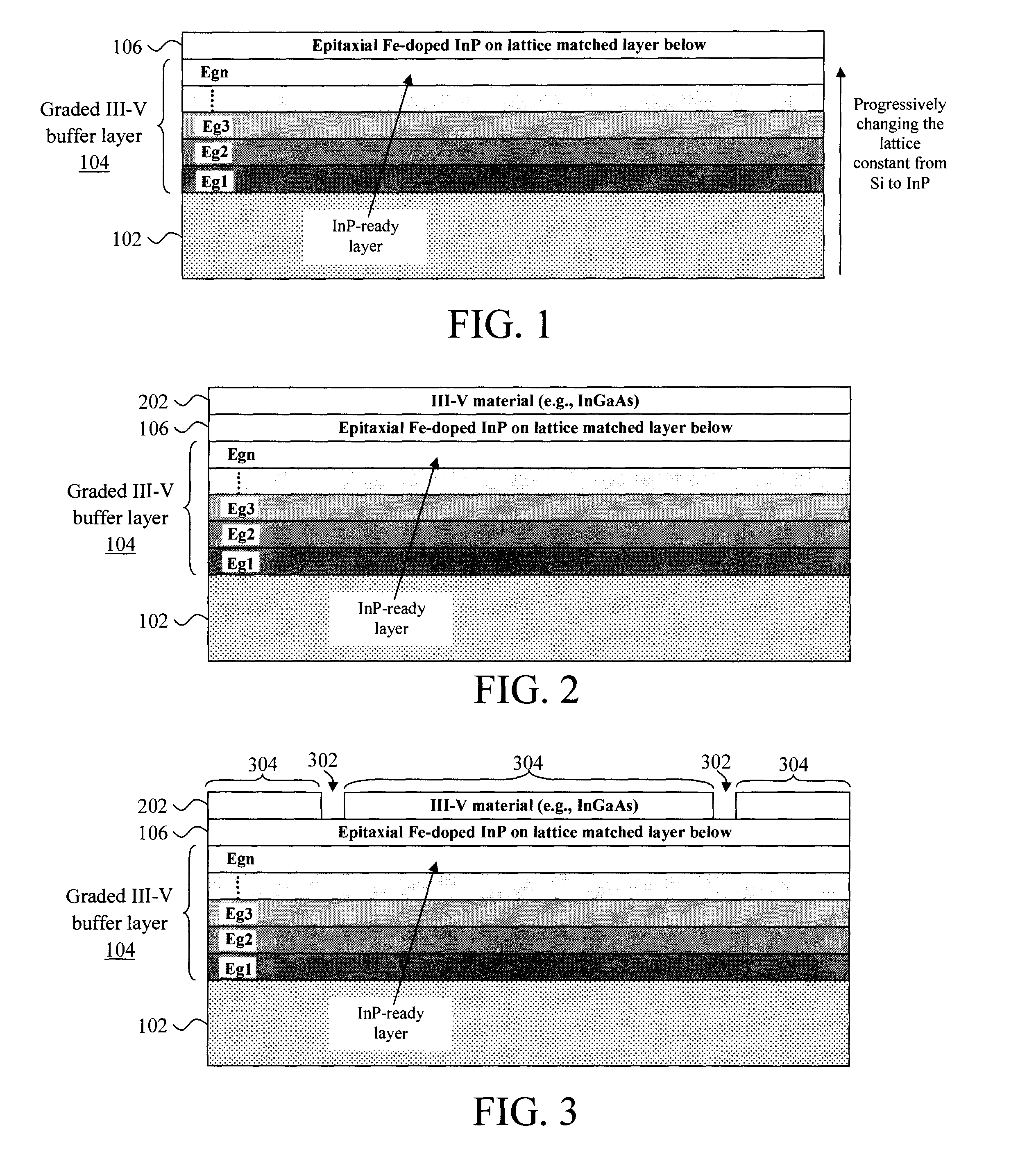
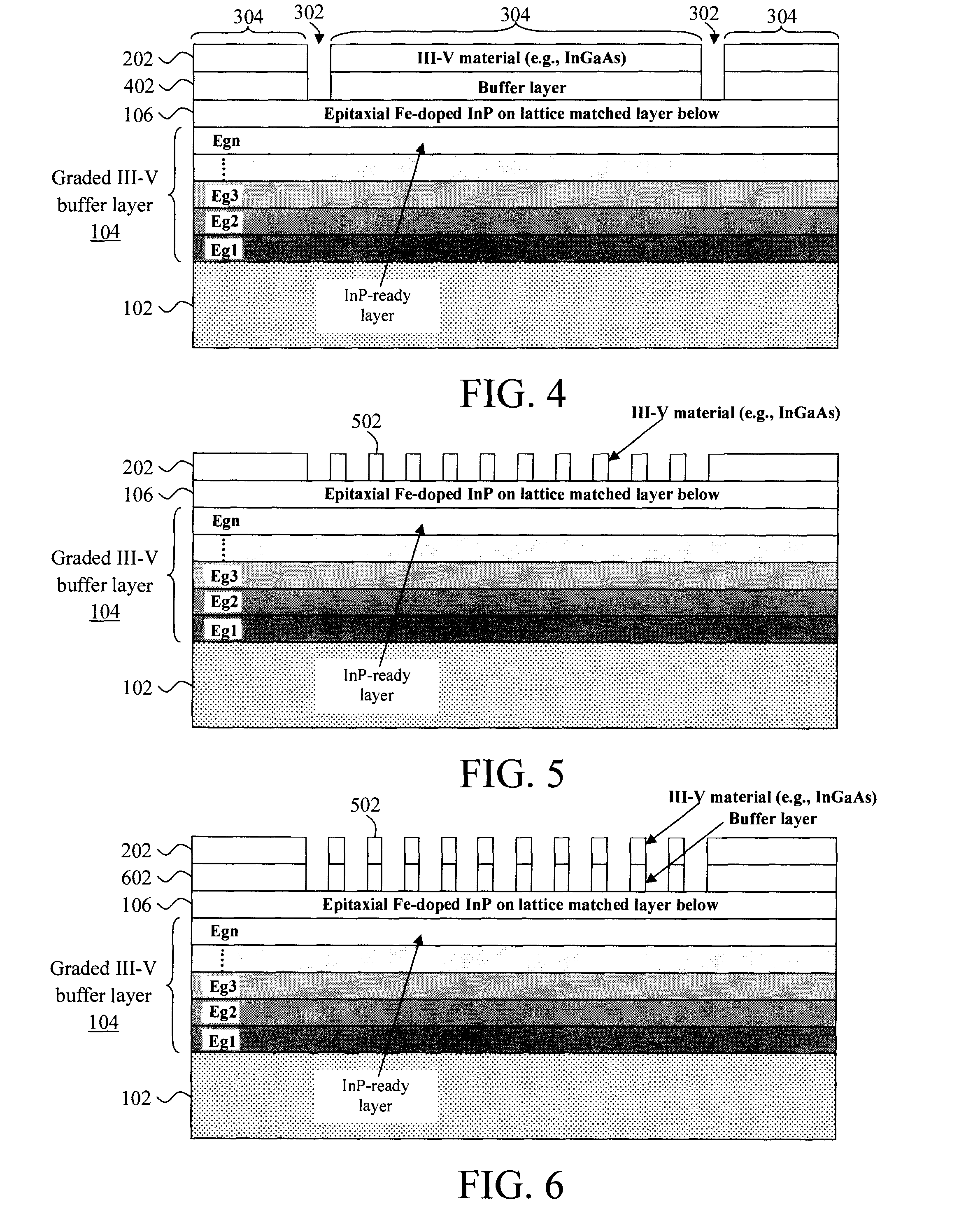
[0016]FIG. 1 is a diagram illustrating an exemplary starting platform for fabricating a III-V semiconductor device, i.e., a device wherein the active area thereof is formed from a III-V semiconductor material. The term “III-V semiconductor material (or simply III-V material), as used herein and throughout the following description, refers to a material that includes at least one group III element and at least one group V element. By way of example only, suitable III-V materials include, but are not limited to, one or more of aluminum gallium arsenide, aluminum gallium nitride, aluminum indium arsenide, aluminum nitride, gallium antimonide, gallium arsenide, gallium nitride, indium antimonide, indium arsenide, indium gallium arsenide, indium gallium nitride, indium nitride, indium phosphide, indium gallium arsenide phosphide (InxGa1-xAsyP1-y) and combinations including at least one of the foregoing materials.

[0017]As described above, lattice mismatch issues have been a challenge for ...


PUM

PropertyMeasurementUnit
resistivityaaaaaaaaaa
thicknessaaaaaaaaaa
resistivityaaaaaaaaaa

Abstract

Techniques for device isolation for III-V semiconductor substrates are provided. In one aspect, a method of fabricating a III-V semiconductor device is provided. The method includes the steps of: providing a substrate having an indium phosphide (InP)-ready layer; forming an iron (Fe)-doped InP layer on the InP-ready layer; forming an epitaxial III-V semiconductor material layer on the Fe-doped InP layer; and patterning the epitaxial III-V semiconductor material layer to form one or more active areas of the device. A III-V semiconductor device is also provided.

Description

FIELD OF THE INVENTION[0001]The present invention relates to III-V semiconductor devices, and more particularly, to techniques for device isolation for III-V semiconductor substrates (such as III-V virtual substrates).BACKGROUND OF THE INVENTION[0002]Lattice mismatch is a factor when forming one material on another, different, material. For instance, when forming epitaxial silicon-germanium (SiGe) on a silicon substrate the crystal lattice of the silicon will serve as a template for the SiGe growth and, even though the SiGe has a larger lattice constant than silicon, the SiGe will conform to the silicon crystal lattice structure. However, this will cause strain in the SiGe layer, and that strain will increase as more SiGe is grown.[0003]For the above-described reasons, the lattice mismatch problem remains a challenge for implementing III-V semiconductor materials in device fabrication that uses heterogeneous epitaxial layers or substrate (e.g., forming III-V epitaxial layers on a si...

Claims


Application Information

Patent Timeline
Patent Type & Authority Applications(United States)
IPC IPC(8): H01L29/205H01L21/3065H01L29/06H01L21/02
CPCH01L29/205H01L21/02543H01L29/0684H01L21/3065H01L21/02546H01L21/02461H01L21/02463H01L21/02488H01L21/02502H01L21/0251H01L21/762H01L29/207H01L21/02241H01L21/02178H01L21/30612H01L21/8252H01L21/823431
Inventor BASU, ANIRBANCOHEN, GUY M.
Owner ELPIS TECH INC
Learn More