Opto-electronic circuit board and method for assembling the same
a technology of optoelectronic circuit boards and components, applied in the direction of optical elements, instruments, optical waveguide light guides, etc., can solve problems such as optical signal distortion, and achieve the effects of accurate and effective signal transmission, reducing optical signal energy loss, and reducing optical signal distortion
- Summary
- Abstract
- Description
- Claims
- Application Information
AI Technical Summary
Benefits of technology
Problems solved by technology
Method used
Image
Examples
first embodiment
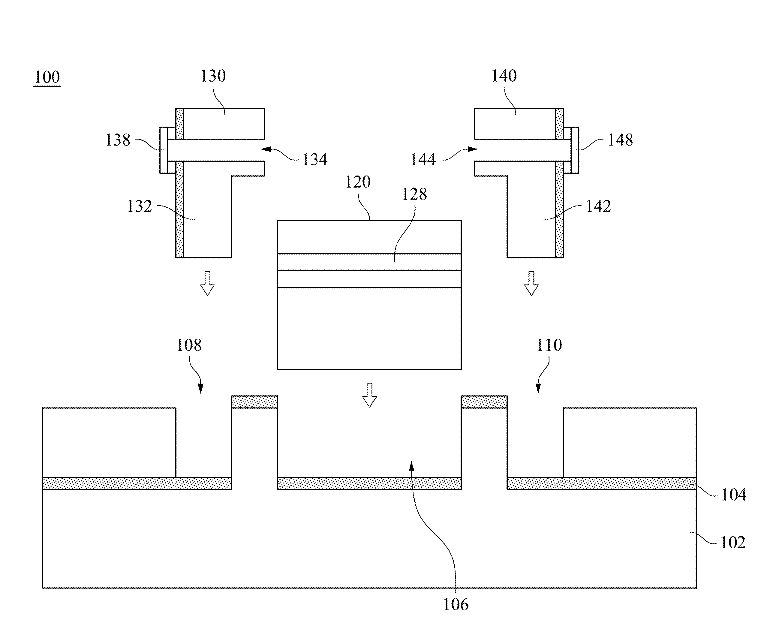
[0070]FIG. 4A is a schematic drawing of assembling an opto-electronic circuit board according to the present invention. In the present embodiment, an opto-electronic circuit board 100 includes a circuit substrate 102, a waveguide 120, an emitting component 130, and a receiving component 140. The circuit substrate 102 includes a first circuit layer 104 and a second circuit layer, and a first cavity 106, a second cavity 108, and a third cavity 110 have already been formed on the circuit substrate 102.
[0071]The waveguide 120 is inserted into the first cavity 106 along a direction of an arrow, in which the size of the waveguide 120 corresponds with the first cavity 106 for inserting. In addition, in order to prevent a loose disposition of the waveguide 120, the size of the waveguide 120 may not be much less than the first cavity 106.
[0072]The emitting component 130 is inserted into the second cavity 108 along a direction of an arrow. The size of the emitting component 130 corresponds wi...
second embodiment
[0093]FIG. 6 is a side view of an opto-electronic circuit board according to the present invention. An opto-electronic circuit board 100 includes a circuit substrate 102, a waveguide 120, an emitting component 130, a receiving component 140, a dielectric layer 160, a surface circuit layer 172, a first blind via 164, a first metal layer 166, a second blind via 168, a second metal layer 170, a first chip 174, and a second chip 176.
[0094]A first reflective layer 150 is disposed on an inner surface of a first light-guide hole 134 of the emitting component 130, and a second reflective layer 152 is disposed on an inner surface of a second light-guide hole 144 of the receiving component 140. The first reflective layer 150 and the second reflective layer 152 are made of a material of gold, copper, nickel, silver, zinc, chromium, tin, aluminum or metal combinations thereof.
[0095]The first reflective layer 150 and the second reflective layer 152 are respectively formed in the fabrications of ...
third embodiment
[0104]FIG. 7 is a side view of an opto-electronic circuit board according to the present invention. A first condenser 154 is disposed between an emitting component 130 and a waveguide 120, and a second condenser 156 is disposed between a receiving component 140 and the waveguide 120. In other words, the first condenser 154 is disposed between the waveguide 120 and the first light-guide hole 134, and the second condenser 156 is disposed between the waveguide 120 and the second light-guide hole 144. A first reflective layer 150 is disposed on an inner surface of the first light-guide hole 134, and a second reflective layer 152 is disposed on an inner surface of the second light-guide hole 144.
[0105]The first condenser 154 and the second condenser 156 provide a focusing effect for an optic signal 139. After a light emitter 138 emits the optic signal 139 to the first condenser 154 through the first light-guide hole 134, the optic signal 139 enters a core layer 128 with focusing on the c...
PUM
| Property | Measurement | Unit |
|---|---|---|
| conductive | aaaaa | aaaaa |
| electrical | aaaaa | aaaaa |
| data transmission speed | aaaaa | aaaaa |
Abstract
Description
Claims
Application Information
 - R&D
- Intellectual Property
- Life Sciences
- Materials
- Tech Scout
- Unparalleled Data Quality
- Higher Quality Content
- 60% Fewer Hallucinations
Browse by: Latest US Patents, China's latest patents, Technical Efficacy Thesaurus, Application Domain, Technology Topic, Popular Technical Reports.
© 2025 PatSnap. All rights reserved.Legal|Privacy policy|Modern Slavery Act Transparency Statement|Sitemap|About US| Contact US: help@patsnap.com


