Passivated porous silicon nanowires

a porous silicon nanowire and passivating technology, applied in electrolytic capacitors, coatings, transportation and packaging, etc., can solve the problems of high cost and cumbersome approach, high cost and cumbersome configuration, and high reactiveness of porous nanowires, so as to achieve the effect of reducing si degradation

Inactive Publication Date: 2015-12-17
RGT UNIV OF CALIFORNIA
View PDF4 Cites 6 Cited by
  • Summary
  • Abstract
  • Description
  • Claims
  • Application Information

AI Technical Summary

Benefits of technology

[0008]It has now been discovered that the surface of Si-based nanowires can be passivated, imparting resistance to degradation during cycling, without substantially diminishing the energy density of the passivated nanowire in comparison to an identical unpassivated nanowire. In various embodiments, the present invention provides porous Si-based nanowires coated with an ultra-thin carbon sheath. The sheath incorporated into the wires of the invention allows full electrolyte access to the porous surface area while still mitigating Si degradation by electrolyte solutions.

Problems solved by technology

For a specific application, a series-parallel configuration is often needed, but can include inherent problems.
This approach is frequently expensive and cumbersome.
The configurations are also large and heavy due to many individual cells used to form the composite structure.
However, these porous nanowires are highly reactive and dissolve rapidly when exposed to mild saline solutions12.
The SiC coatings were 10's of nm thick and, while they successfully mitigated Si degradation during electrochemical cycling in aqueous electrolytes, they also resulted in pore blockage and a large decrease in the materials' energy storage potential
In spite of extensive research and effort, making robust supercapacitors with high energy and power density still remains challenging.
Supercapacitor electrodes of the prior art have not provided the device performance (e.g., energy density, power density, cycling stability, operating voltage) and manufacturability required for many high-performance, commercial applications.

Method used


Image

  • Passivated porous silicon nanowires
  • Passivated porous silicon nanowires
  • Passivated porous silicon nanowires

Examples


example 1

Materials and Methods

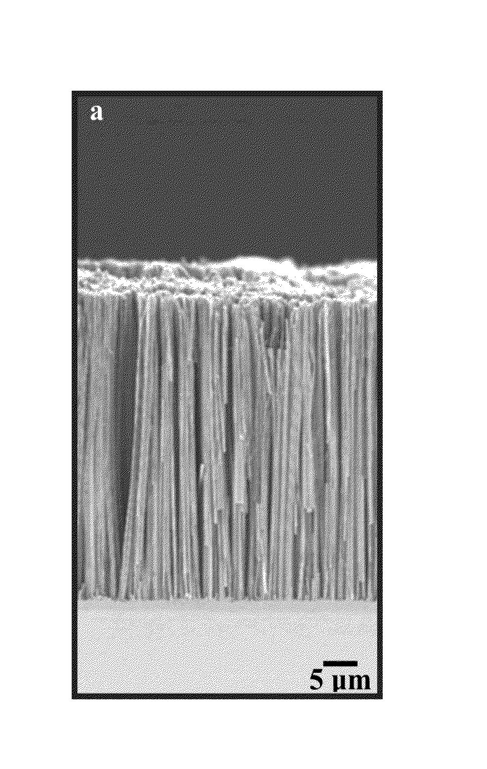
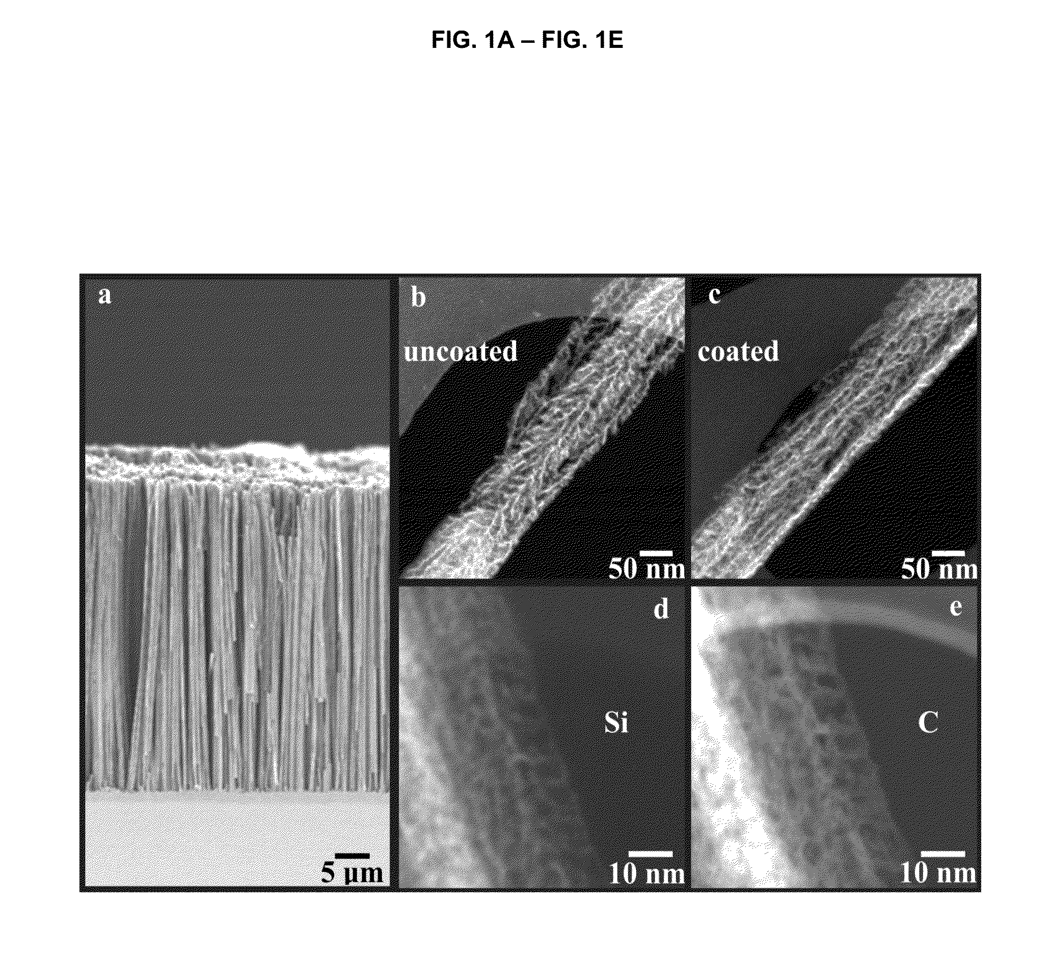
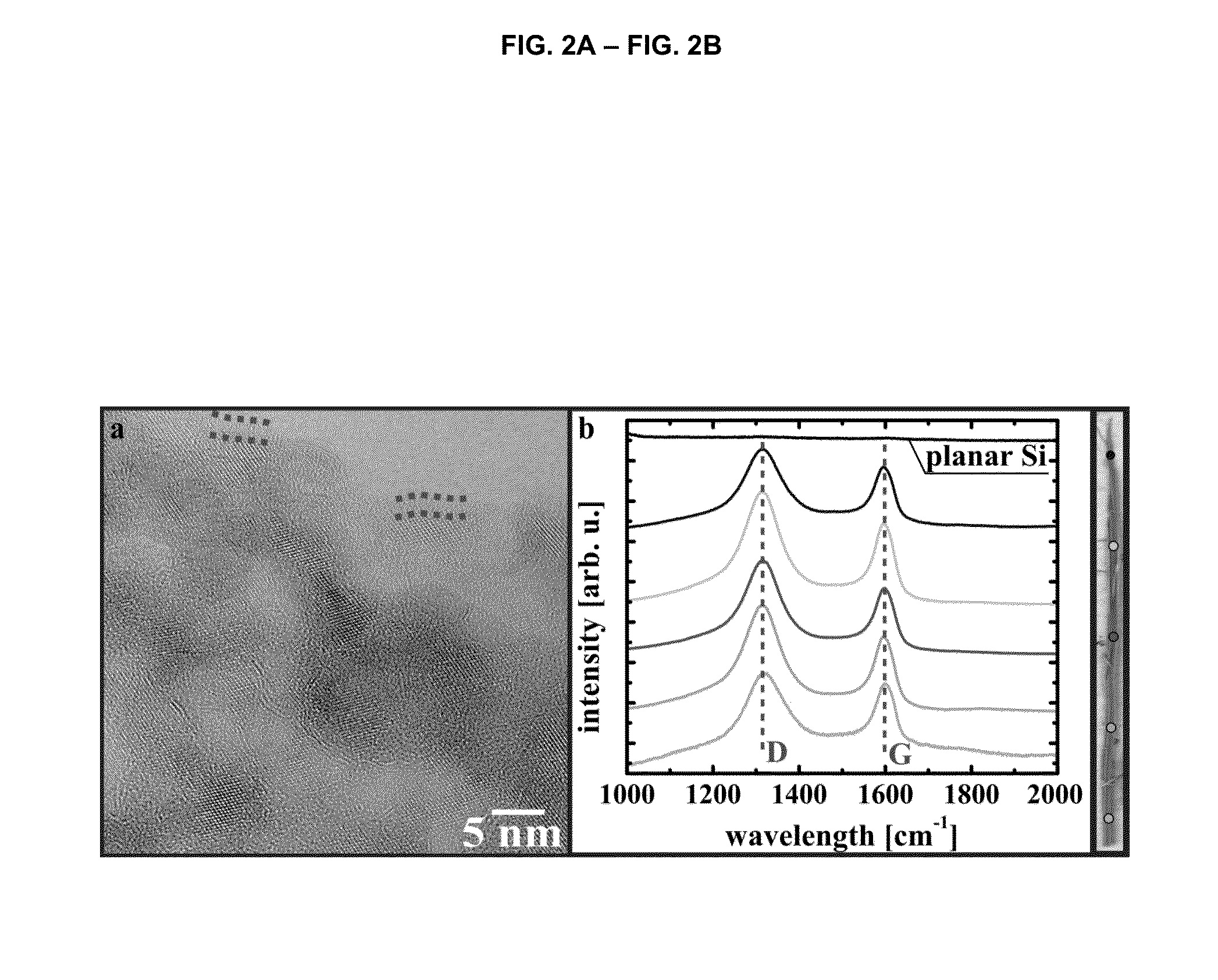
[0066]Porous SiNWs were synthesized following the previously published method8. 1×1 cm2 (1-5 mΩ·cm) silicon (100) coupons were cleaned by successive sonication in acetone, isopropyl alcohol and de-ionized water. The coupons were then exposed to UV generated ozone for 5 minutes and any silicon oxide was subsequently removed by a 5 minute etch in 48% hydrofluoric acid (HF). The unpolished sides of the samples were coated with a thin nylon coating in order to protect them from etching. A ˜2 mm wide strip of Si on the front side of the samples was also protected to provide an electrical contact point. Samples were then immersed in the oxidant / etchant bath consisting of 5M HF and 20 mM AgNO3, equilibrated in a 50° C. heating bath, for various lengths of time to produce different length wire arrays. Samples were then rinsed in de-ionized water and residual silver was removed by a HNO3 (˜3.5M) etch for 15-45 minutes. Drying was performed in a critical point dryer (Tous...


PUM

PropertyMeasurementUnit
lengthaaaaaaaaaa
thicknessaaaaaaaaaa
diameteraaaaaaaaaa

Abstract

In exemplary embodiments, there is provided a scalable process for producing supercapacitor electrodes with very high specific capacitance and specific energy density, and very high capacitance retention after thousands of charge discharge cycles. The electrode material consists of a thin, electrically conductive carbon coating deposited onto nanoporous silicon nanowires. The coating prevents degradation of the silicon nanowires in aqueous solutions, while leaving the pore area fully accessible, enabling application as a supercapacitor electrode with the highest capacitance per projected area to date. The nanowires also are of use as a water splitting electrode and aqueous fuel cell electrode.

Description

CROSS REFERENCE TO RELATED APPLICATIONS[0001]The present application claims priority under 35 U.S.C. §119(e) to U.S. Provisional Patent Application No. 62 / 010,909 filed Jun. 11, 2014, which is incorporated herein by reference in its entirety.STATEMENT OF GOVERNMENT RIGHTS[0002]This invention was made with U.S. Government support under Grants Nos. EEC-0832819 (Center of Integrated Nanomechanical Systems) and DMR-1207053, awarded by the National Science Foundation. The Government has certain rights in the invention.BACKGROUND OF THE INVENTION[0003]Supercapacitors function by storing electrical charge (Q) in the electrochemical double layer at the interface between an electrode and an electrolyte. When the electrode is biased with a potential V, ions of the opposite charge are electrostatically attracted to the electrode surface, forming the ECDL and leading to a capacitance, C, described by the standard parallel plate capacitor equation C=A / d∈1. Here A is the interfacial area of the e...

Claims


Application Information

Patent Timeline
Patent Type & Authority Applications(United States)
IPC IPC(8): H01G11/36H01G11/86
CPCH01G11/86H01G11/36H01G11/30Y02E60/13Y02T10/70
Inventor MABOUDIAN, ROYAALPER, JOHN P.CARRARO, CARLO
Owner RGT UNIV OF CALIFORNIA
Why Eureka
Try Eureka