Inductor element, inductor bridge, and high-frequency filter
a technology of inductance bridge and inductance element, which is applied in the direction of inductance, multiple-port network, resonance antenna, etc., to achieve the effect of reducing direct-current resistance (dcr), reducing interline capacitance and interlayer capacitance, and reducing line length
- Summary
- Abstract
- Description
- Claims
- Application Information
AI Technical Summary
Benefits of technology
Problems solved by technology
Method used
Image
Examples
first preferred embodiment
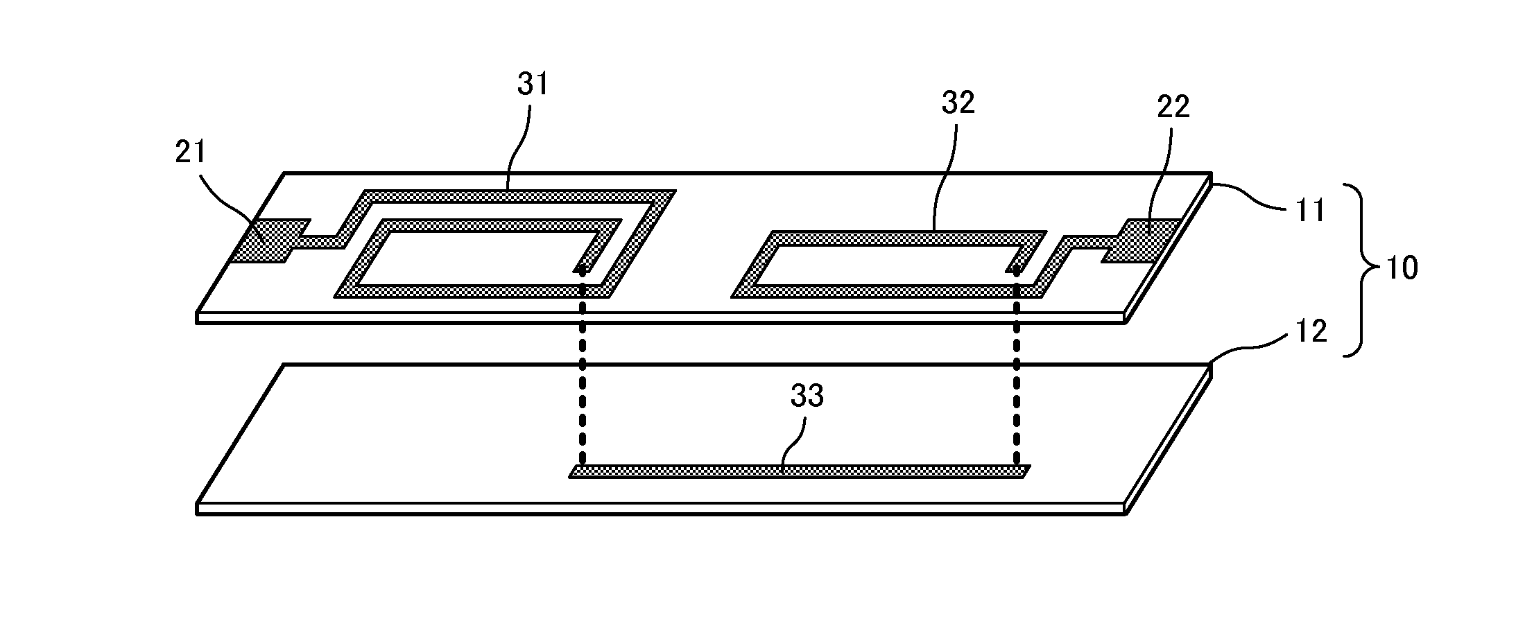
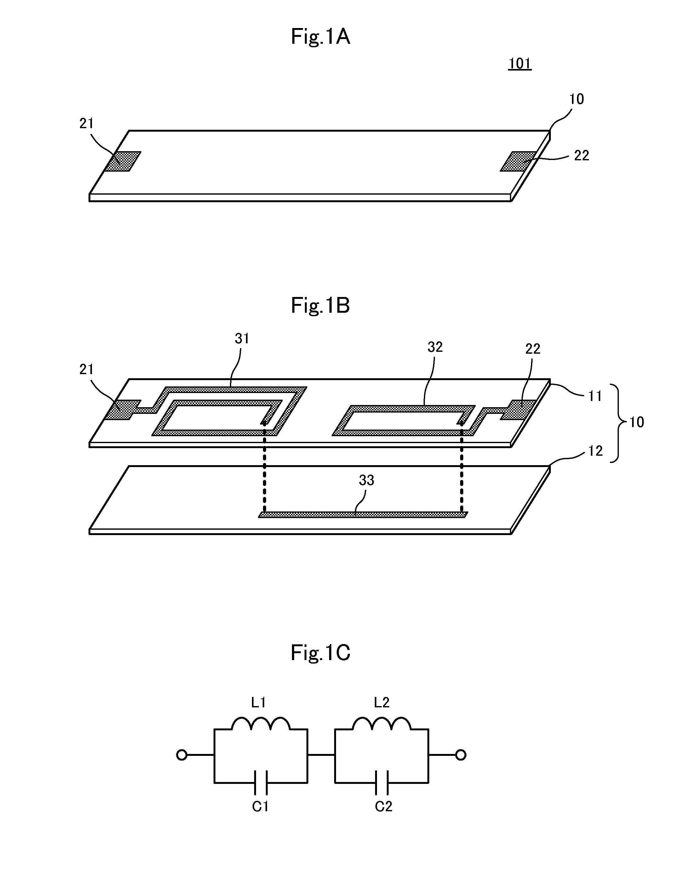
[0038]FIG. 1A is a perspective view illustrating the appearance of an inductor element 101 according to a first preferred embodiment of the present invention. FIG. 1B is an exploded perspective view of the inductor element 101. It should be noted, however, that a resist film is not illustrated in FIG. 1B. FIG. 1C is an equivalent circuit diagram of the inductor element 101 according to the first preferred embodiment.
[0039]The inductor element 101 includes an element body 10 and terminal electrodes 21 and 22 provided on the element body 10, and is used with the terminal electrodes 21 and 22 connected to a predetermined circuit. The inductor element is preferably configured for use as a high-frequency filter, in particular a band rejection filter or a low-pass filter, for example.
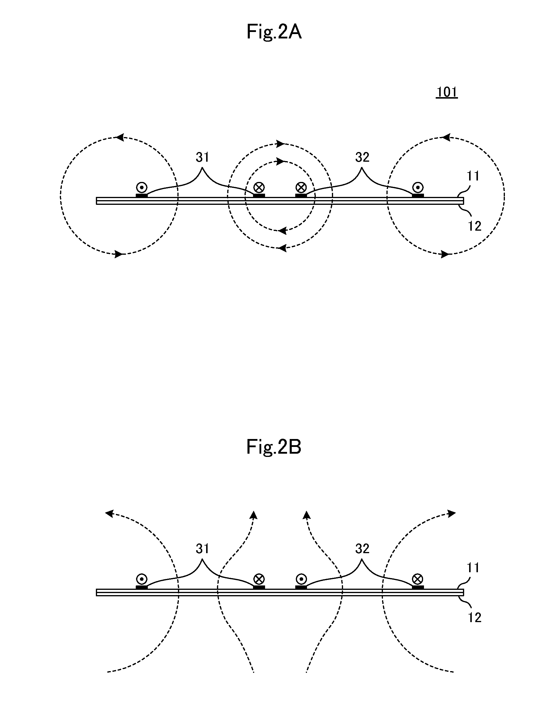
[0040]As illustrated in FIG. 1B, the element body 10 is formed preferably by stacking resin substrates 11 and 12 made of a liquid crystal polymer (LCP), for example. Rectangular-spiral (coil-shaped) conductor...
second preferred embodiment
[0063]FIG. 8 is an exploded perspective view of an inductor element 102 according to a second preferred embodiment of the present invention. The inductor element 102 includes an element body 10 and terminal electrodes 21 and 22 provided on the element body 10, and is used with the terminal electrodes 21 and 22 connected to a predetermined circuit.
[0064]As illustrated in FIG. 8, the element body 10 is formed preferably by stacking resin substrates 11 and 12 made of a liquid crystal polymer (LCP), for example. Rectangular-spiral (coil-shaped) conductor patterns 31, 32, 34, and 35 are provided on the resin substrate 11. Coils defined by the conductor patterns 31, 32, 34, and 35 each have a coil axis that extends in a direction that is perpendicular or substantially perpendicular to a surface of the resin substrate 11 (in a direction that is perpendicular or substantially perpendicular to the principal surface of the element body 10).
[0065]Line-segment conductor patterns 33 and 36 are p...
third preferred embodiment
[0068]A third preferred embodiment of the present invention provides an example of a high-frequency circuit module that includes an inductor element. FIG. 9 is a perspective view of a circuit substrate 200 and a high-frequency circuit module 110 disposed in a housing of an electronic device.
[0069]The high-frequency circuit module 110 includes a resin substrate made of a liquid crystal polymer (LCP). An antenna portion 110a, a component mounting portion 110b, and an inductor portion 110c are defined by an integral stacked body. The antenna portion 110a includes an antenna element pattern 91 provided on the element body 10, and defines and functions as a multi-band antenna. The component mounting portion 110b includes components such as a radio-frequency integrated circuit (RFIC) mounted on the element body 10 to define a high-frequency circuit. The inductor portion 110c includes conductor patterns that are similar to the conductor patterns illustrated in FIG. 8 to define and function...
PUM
| Property | Measurement | Unit |
|---|---|---|
| interior angle | aaaaa | aaaaa |
| frequency | aaaaa | aaaaa |
| self-resonant frequency | aaaaa | aaaaa |
Abstract
Description
Claims
Application Information
 - R&D
- Intellectual Property
- Life Sciences
- Materials
- Tech Scout
- Unparalleled Data Quality
- Higher Quality Content
- 60% Fewer Hallucinations
Browse by: Latest US Patents, China's latest patents, Technical Efficacy Thesaurus, Application Domain, Technology Topic, Popular Technical Reports.
© 2025 PatSnap. All rights reserved.Legal|Privacy policy|Modern Slavery Act Transparency Statement|Sitemap|About US| Contact US: help@patsnap.com


