MEMS Fabrication Process with Two Cavities Operating at Different Pressures

a technology of mems and cavity, applied in the direction of fluid speed measurement, acceleration measurement using interia forces, instruments, etc., can solve the problems of large footprint of combined sensor circuits, conflicting processing steps, and unsuitability of first sensor vacuum, and the gyroscope sensor may not be suitable for another sensor. , the gyroscope wafer cavity getter material used to form vacuum in gyroscope wafer can impose additional expense and processing constraints

Active Publication Date: 2015-12-31
NXP USA INC
View PDF0 Cites 30 Cited by
  • Summary
  • Abstract
  • Description
  • Claims
  • Application Information

AI Technical Summary

Problems solved by technology

With existing semiconductor processing techniques, there are challenges with integrating multiple MEMS sensors onto a single integrated circuit device, such as when different MEMS sensors operating at different cavity pressures are separately fabricated and assembled into a single substrate layer, resulting in a combined sensor circuit having a large footprint and potentially conflicting processing steps.
For example, the bonding techniques used to form a good vacuum for a first sensor (e.g., gyroscope sensor) may be unsuitable for another sensor (e.g., an overdamped accelerometer) ...

Method used


Image

  • MEMS Fabrication Process with Two Cavities Operating at Different Pressures
  • MEMS Fabrication Process with Two Cavities Operating at Different Pressures
  • MEMS Fabrication Process with Two Cavities Operating at Different Pressures

Examples


Embodiment Construction

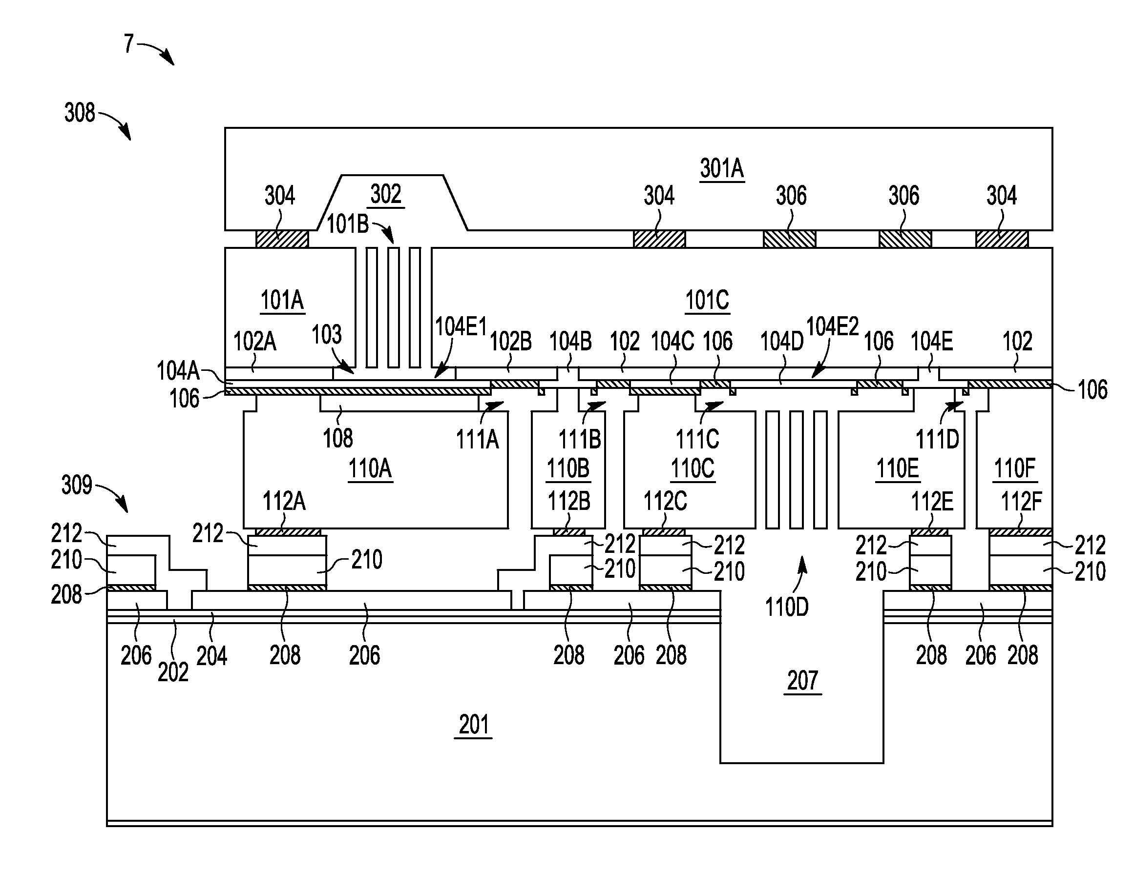
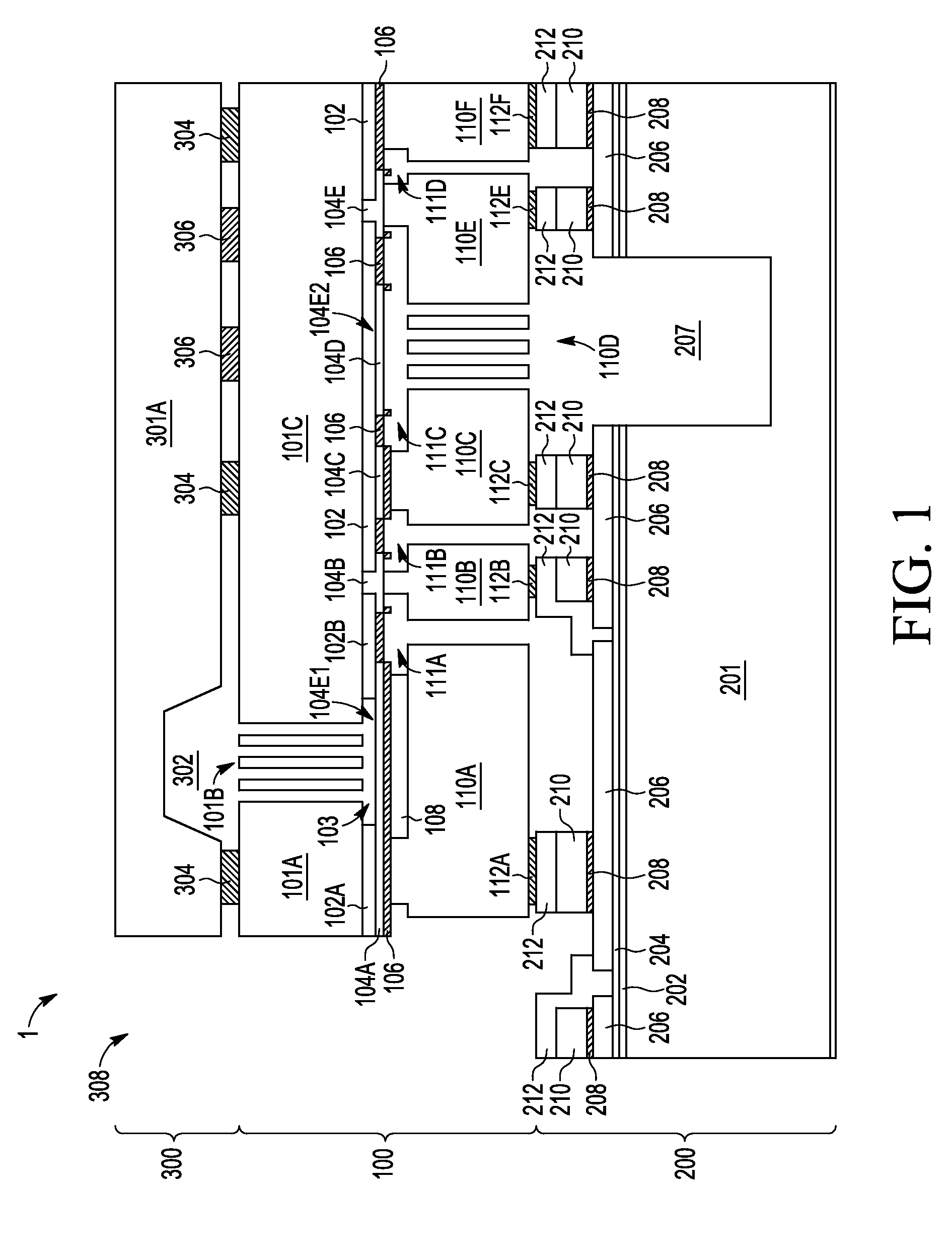
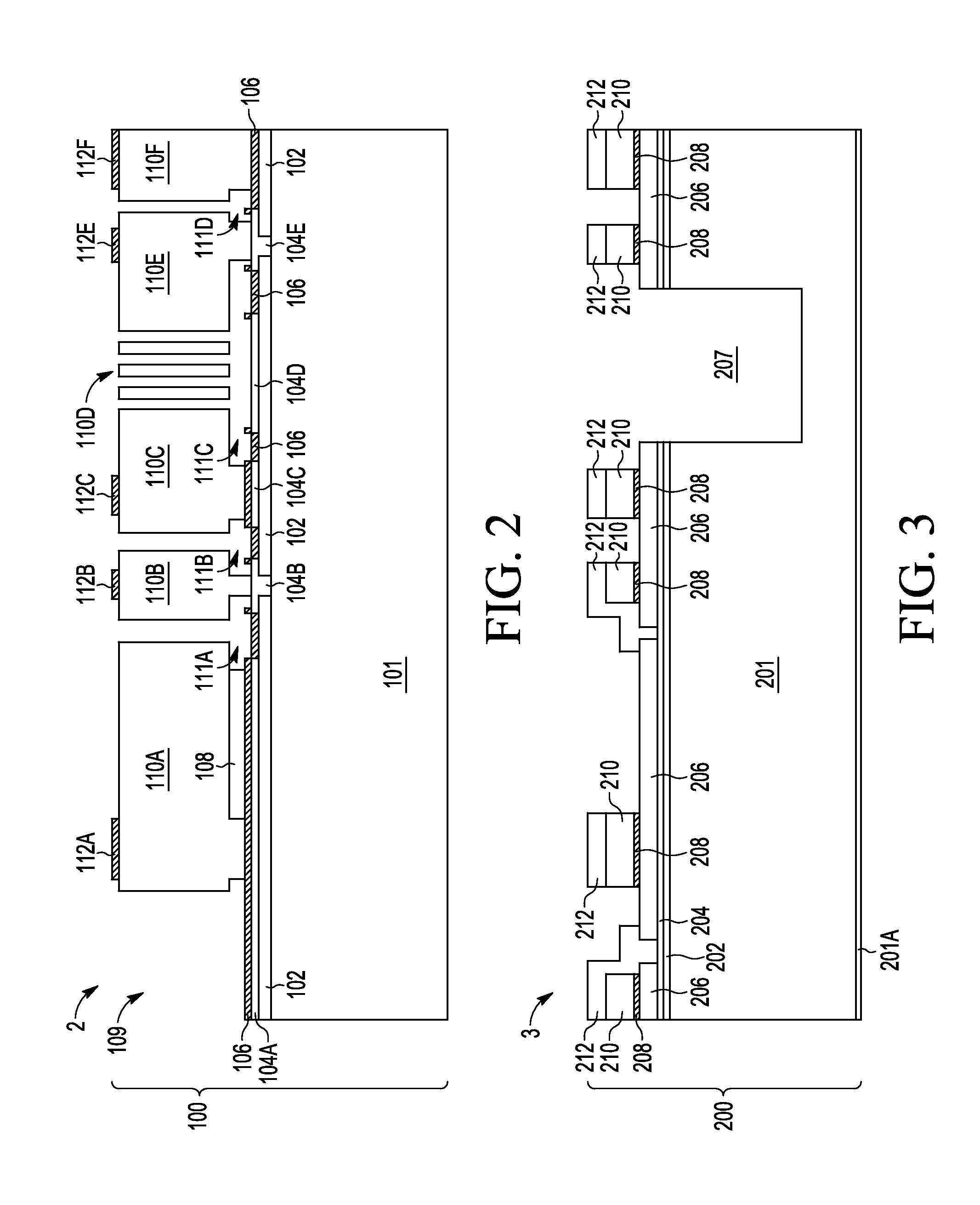
[0008]A method and apparatus are described for fabricating a plurality of high aspect ratio transducers in a vertically stacked MEMS device wafer assembly by applying separate transducer etch processes to different assembly layers that may be attached into a single MEMS device wafer assembly using different wafer bonding techniques. In selected embodiments, a first MEMS device wafer having a deposited polycrystalline semiconductor layer and a first monocrystalline substrate is subjected to a first transducer etch process of the poly layer to form interconnects, bond and sealing ring structures, and the movable mass used for a first MEMS sensor (e.g., a gyroscope sensor mass). As will be appreciated, additional processing may be used to form one or more sensor electrodes, driver electrodes, and / or interconnect routing in the first MEMS device. In addition, a first patterned conductor layer (e.g., germanium) may be formed on the first MEMS device wafer for use in forming a bond (e.g.,...


PUM

PropertyMeasurementUnit
Temperatureaaaaaaaaaa
Pressureaaaaaaaaaa
Electrical conductivityaaaaaaaaaa

Abstract

A method and apparatus are described for fabricating a high aspect ratio MEMS sensor device having multiple vertically-stacked inertial transducer elements (101B, 110D) formed in different layers of a multi-layer semiconductor structure (100) and one or more cap devices (200, 300) bonded to the multi-layer semiconductor structure (100) to protect any exposed inertial transducer element from ambient environmental conditions.

Description

BACKGROUND OF THE INVENTION[0001]1. Field of the Invention[0002]The present invention is directed in general to the field of semiconductor devices. In one aspect, the present invention relates to MEMS devices and methods for fabricating MEMS devices.[0003]2. Description of the Related Art[0004]Micro-Electro-Mechanical Systems (MEMS) technology is increasingly used to integrate mechanical elements, sensors, actuators, and electronics on a common silicon substrate through microfabrication technology. For example, inertial sensors may be formed with MEMS devices on an integrated circuit wafer substrate to form various applications, such accelerometers for measuring linear acceleration, gyroscopes for measuring angular velocity, optical devices, pressure sensors, switches, and so forth. A conventional MEMS device typically includes a moveable element, such as a proof mass, diaphragm, mirror, and the like that is flexible or movable, and is attached to the rest of the device. Relative mo...

Claims


Application Information

Patent Timeline
IPC IPC(8): B81B7/00B81C1/00
CPCB81C1/00238B81B2201/0235B81B2201/0242B81C1/00246B81C1/00253
Inventor STEIMLE, ROBERT F.WINEBARGER, PAUL M.
Owner NXP USA INC
Why Eureka
Try Eureka