Planar beam forming and steering optical phased array chip and method of using same

a phased array and chip technology, applied in optics, wave based measurement systems, instruments, etc., can solve the problems of low yield, cost, and/or different yield of two-dimensional beam forming and steering phased arrays in the optical domain that are produced to date, and achieve low cost and high yield

Active Publication Date: 2015-12-31
QUANERGY SOLUTIONS INC
View PDF5 Cites 177 Cited by
  • Summary
  • Abstract
  • Description
  • Claims
  • Application Information

AI Technical Summary

Benefits of technology

[0007]A one-dimensional (1D) planar beam forming and steering optical phased array chip is a simple building block of a two-dimensional (2D) beam forming and steering solid-state lidar, enabling manufacturing of said lidars at high yield and low cost through the use of a plurality of said chips. Innovative Photonic Integrated Circuit (PIC) chip architectures that follow Design for Manufacturing (DFM) rules enable said building blocks.

Problems solved by technology

Phased arrays in the optical domain that are produced to date are complex, costly and / or have a different purpose than beam forming and beam steering; some combine spatial filters, optical amplifiers and ring lasers (U.S. Pat. No. 7,339,727), some involve a plurality of optical input beams (U.S. Pat. No. 7,406,220), some involve volume diffraction gratings and a plurality of input directions (U.S. Pat. No. 7,428,100), some combine beams of a plurality of wavelengths (U.S. Pat. No. 7,436,588), some have optical phase reference sources and gain elements (U.S. Pat. No. 7,489,870), some have predetermined areas in the field of view and a plurality of beam forming elements (U.S. Pat. No. 7,532,311), and some have multiple frequencies and multiple optical phase reference sources (U.S. Pat. No. 7,555,217).
Two-dimensional beam forming and steering phased arrays in the optical domain that are produced to date have low yields and are costly because they steer in two dimensions with a complex two-dimensional pixel array.

Method used


Image

  • Planar beam forming and steering optical phased array chip and method of using same
  • Planar beam forming and steering optical phased array chip and method of using same
  • Planar beam forming and steering optical phased array chip and method of using same

Examples


Embodiment Construction

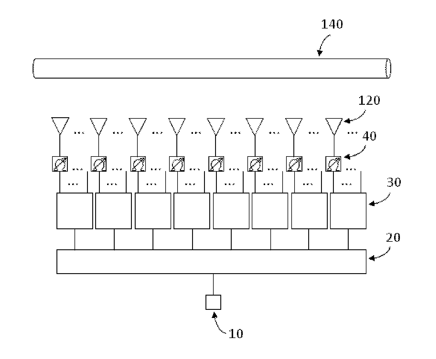
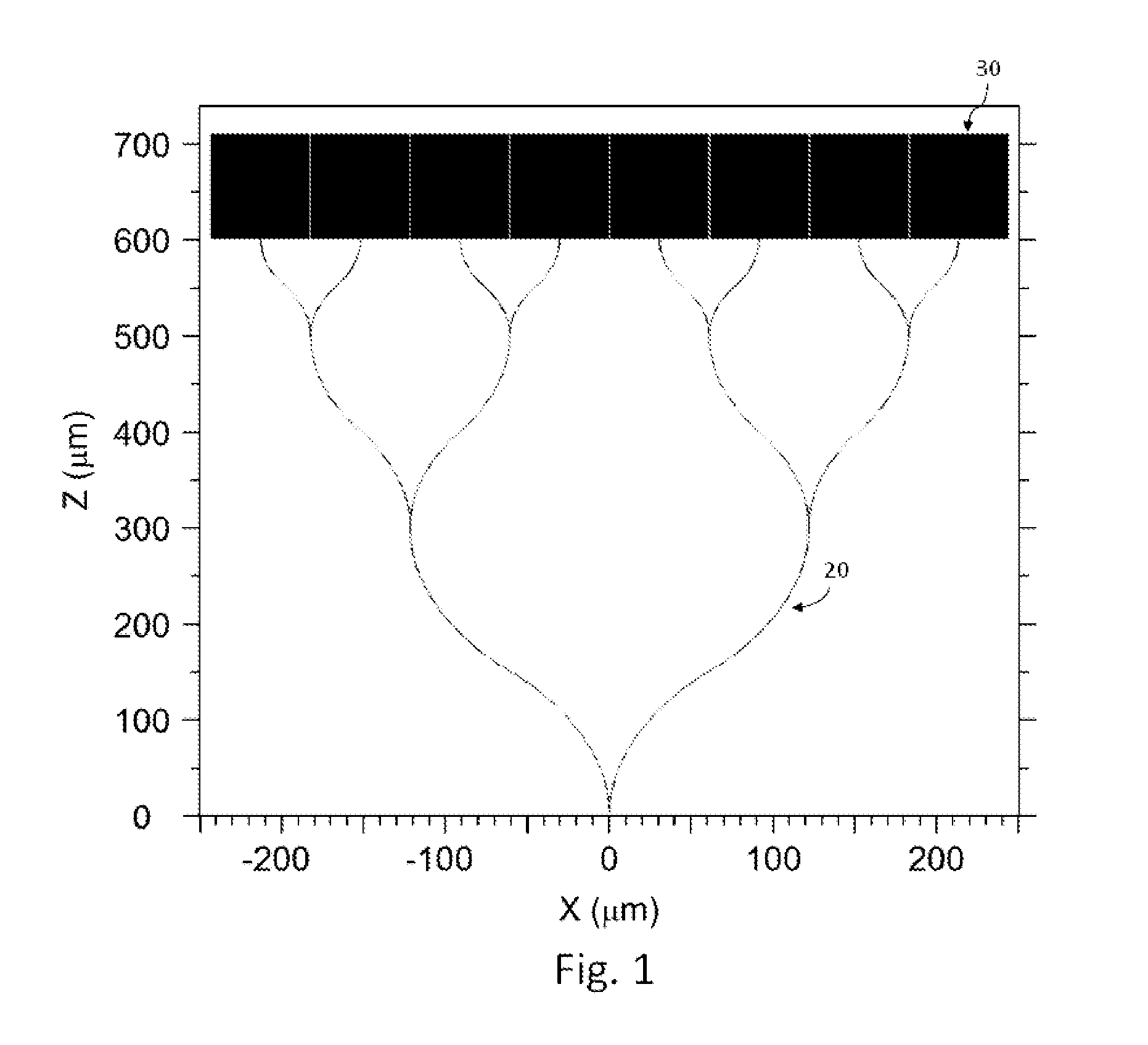
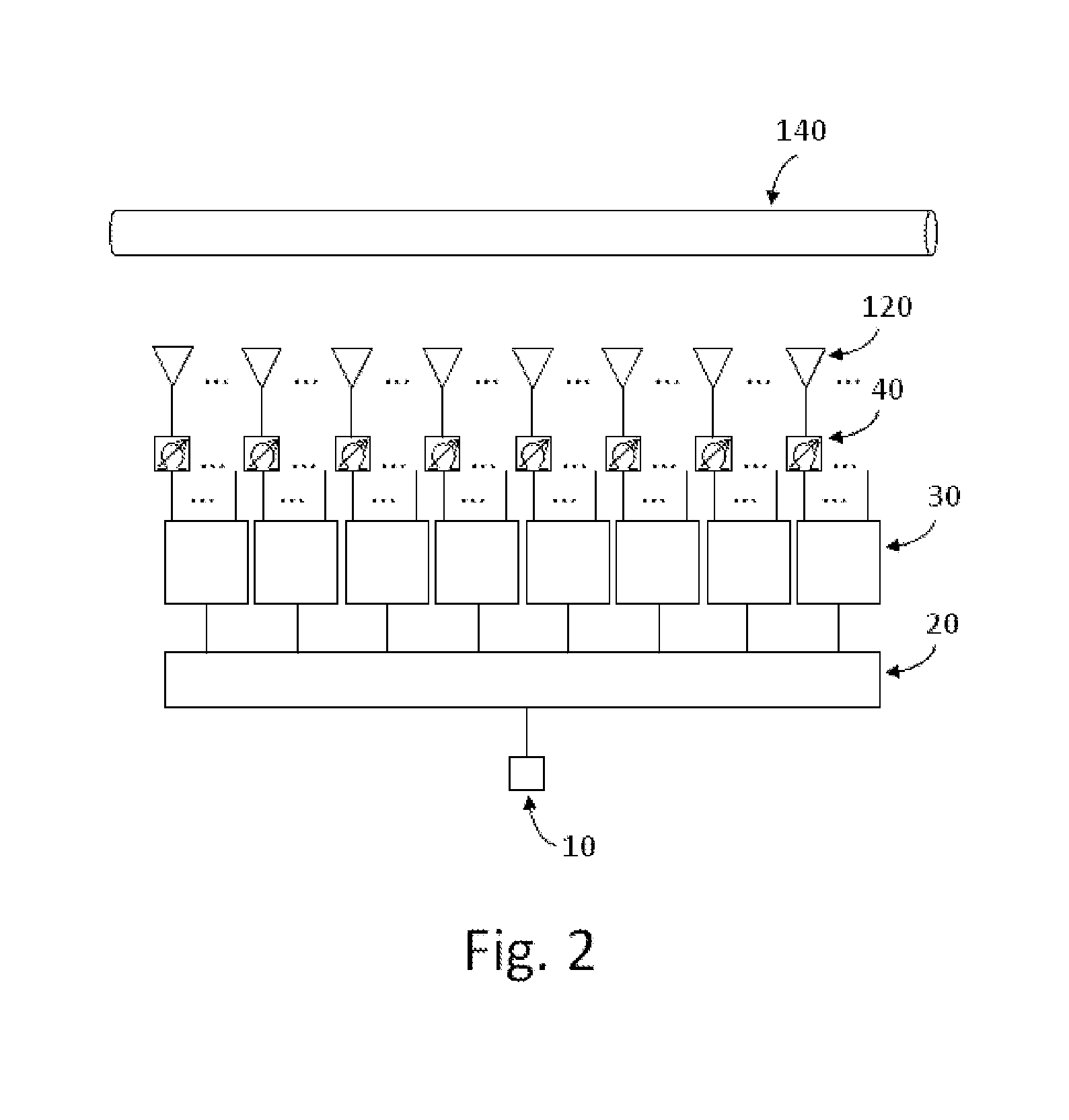
[0017]A lidar-based apparatus and method are used for the solid state steering of laser beams using Photonic Integrated Circuits (PICs). Integrated optic design and fabrication micro- and nanotechnologies are used for the production of chip-scale optical splitters that distribute an optical signal from a laser essentially uniformly to an array of pixels, said pixels comprising tunable optical delay lines and optical antennas. Said antennas achieve out-of-plane coupling of light.

[0018]As the delay lines of said antenna-containing pixels in said array are tuned, each antenna emits light of a specific phase to form a desired far-field radiation pattern through interference of these emissions. Said array serves the function of solid state optical phased array (OPA).

[0019]By incorporating a large number of antennas, high-resolution far-field patterns can be achieved by an OPA, supporting the radiation pattern beam forming and steering needed in solid state lidar, as well as the generatio...


PUM

PropertyMeasurementUnit
spot sizeaaaaaaaaaa
optical power splittingaaaaaaaaaa
phase shifteraaaaaaaaaa

Abstract

A one-dimensional planar beam forming and steering optical phased array chip is a simple building block of a two-dimensional beam forming and steering solid-state lidar, enabling manufacturing of said lidars at high yield and low cost through the use of a plurality of said chips. Innovative photonic integrated circuit chip architectures that follow design for manufacturing rules enable said building blocks.

Description

REFERENCES CITEDU.S. Patent Documents7,339,727 B1 March 2008 Rothenberg7,406,220 B1 July 2008 Christensen7,428,100 B2 September 2008 Smith7,436,588 B2 October 2008 Rothenberg7,489,870 B2 February 2009 Hillis7,532,311 B2 May 2009 Henderson7,555,217 B2 July 2009 HillisFIELD OF THE INVENTION[0001]The present invention relates generally to the field of environment sensing, and more particularly to the use of Time of Flight (ToF) lidar sensors for real-time three-dimensional mapping and object detection, tracking, identification and / or classification.BACKGROUND OF THE INVENTION[0002]A lidar sensor is a light detection and ranging sensor. It is an optical remote sensing module that can measure the distance to a target or objects in a scene, by irradiating the target or scene with light, using pulses (or alternatively a modulated signal) from a laser, and measuring the time it takes photons to travel to said target or landscape and return after reflection to a receiver in the lidar module....

Claims


Application Information

Patent Timeline
Patent Type & Authority Applications(United States)
IPC IPC(8): G02F1/29G02B17/00G02F1/295G02B5/32G02B3/00G02B27/42
CPCG02F1/292G01S7/4813G01S7/4817G01S7/4814
Inventor ELDADA, LOUAY
Owner QUANERGY SOLUTIONS INC
Why Eureka
Try Eureka