

Light receiving device including transparent electrode and method of manufacturing light receiving device
- Summary
- Abstract
- Description
- Claims
- Application Information
AI Technical Summary
Benefits of technology
Problems solved by technology
Method used
Image

Examples
Embodiment Construction
[0034]Hereinafter, exemplary embodiments of the present invention will be described with reference to the attached drawings.
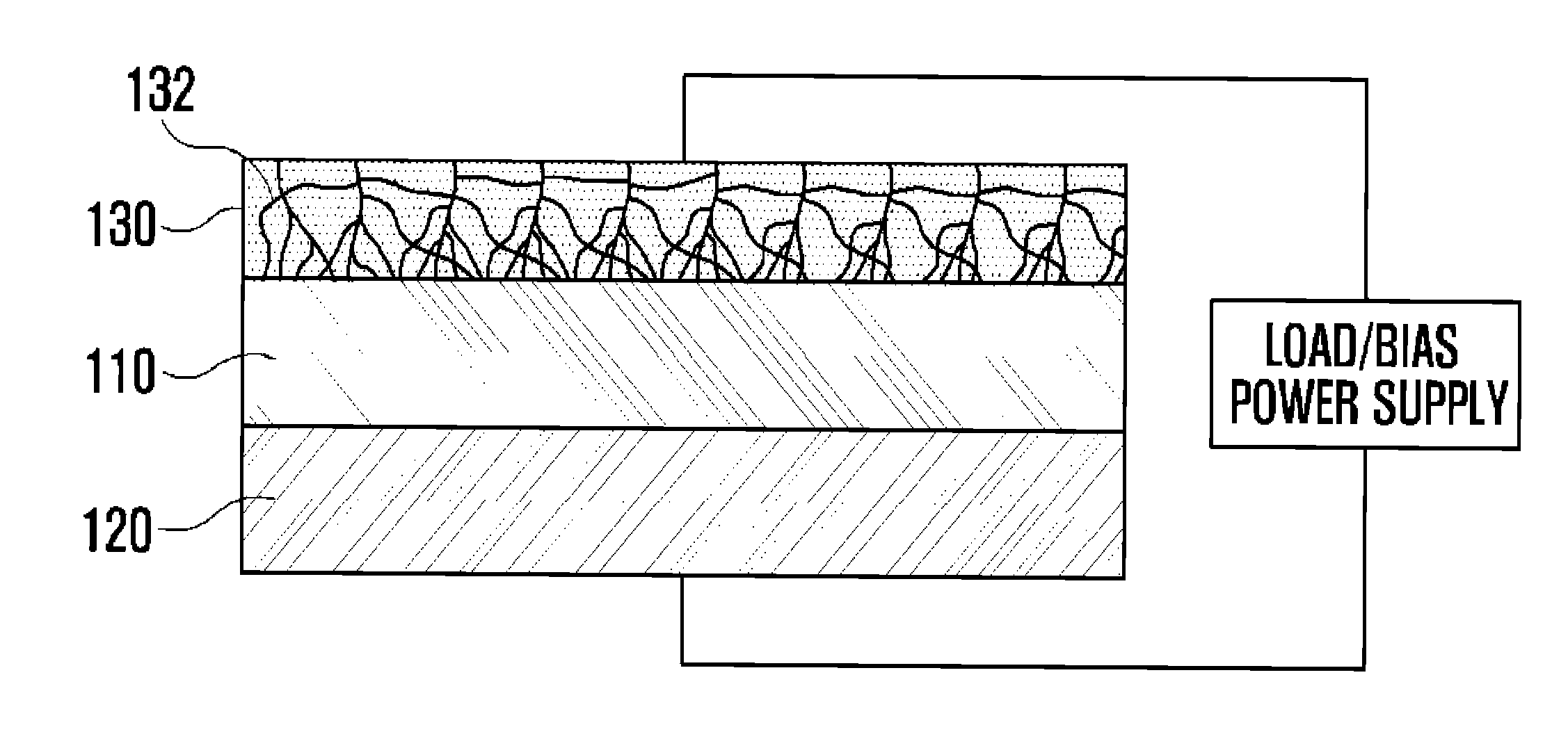
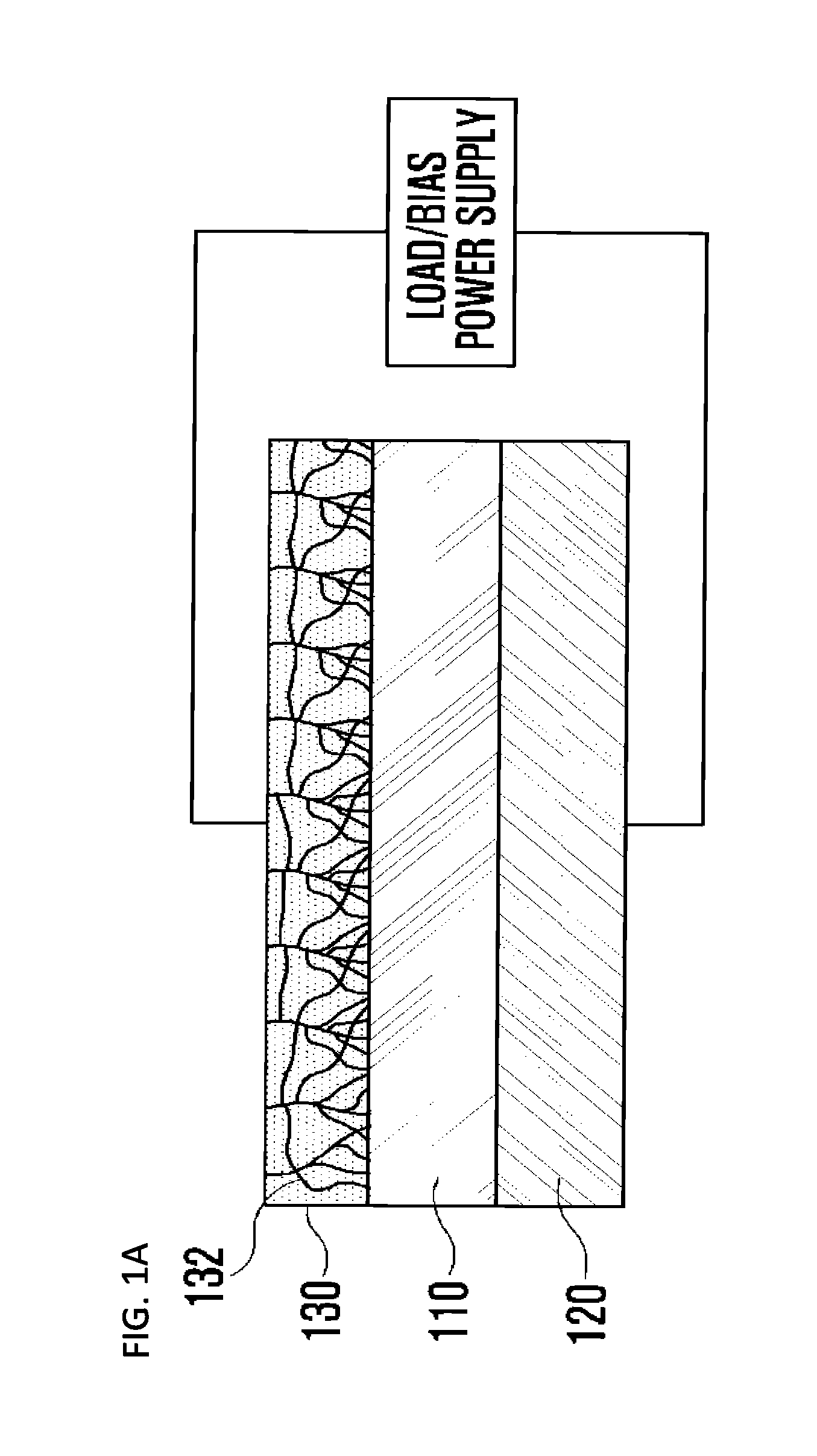
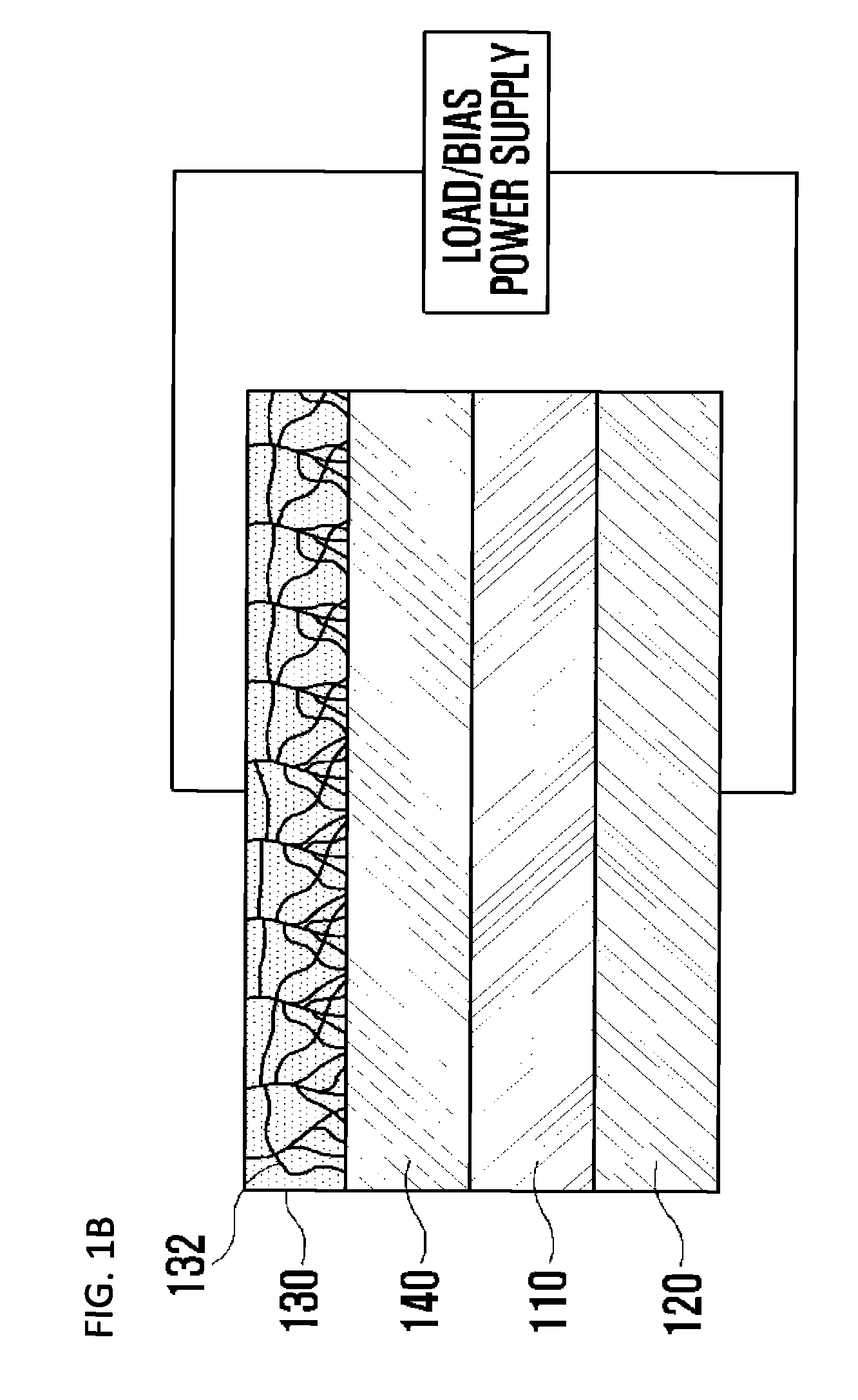
[0035]FIG. 1a is a diagram illustrating a configuration of a light receiving device including a transparent electrode 130 according to an embodiment of the present invention.
[0036]Referring to FIG. 1a, the light receiving device according to the embodiment of the present invention is configured so that a photoelectric conversion layer 110 which absorbs light to converts the light into electric energy is interposed between a transparent electrode 130 and an opposite electrode 120.
[0037]The photoelectric conversion layer 110 absorbs light and generates electron-hole pairs to converts optical energy into electric energy according to the photoelectric conversion effect. The light receiving device may be implemented in various structures, for example, a PN junction structure or a PIN layer structure. In the PIN layer structure, a p-type semiconductor layer and an n-...
PUM
 Abstract
Description
Claims
Application Information