A kind of preparation method of alpha phase gallium oxide thin film

A phase gallium oxide thin film technology, which is applied in the field of preparation of alpha phase gallium oxide thin film, can solve the problem of low film formation rate and achieve the effect of uniform particle size distribution, smooth surface and large area

Active Publication Date: 2022-07-05
NANJING UNIV OF INFORMATION SCI & TECH
View PDF4 Cites 0 Cited by
  • Summary
  • Abstract
  • Description
  • Claims
  • Application Information

AI Technical Summary

Problems solved by technology

Currently used to prepare α-Ga 2 o 3 The methods of materials mainly include mist chemical vapor deposition (mist-CVD), halide vapor phase epitaxy (HVPE), molecular beam epitaxy (MBE) and atomic layer deposition (ALD), among which mist-CVD and HVPE are chemical methods, which are easy Introduce impurities, MBE and ALD method film formation rate is low

Method used


Image

  • A kind of preparation method of alpha phase gallium oxide thin film
  • A kind of preparation method of alpha phase gallium oxide thin film
  • A kind of preparation method of alpha phase gallium oxide thin film

Examples


Embodiment 1

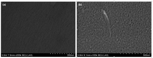
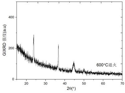
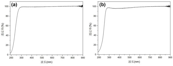
[0024] The preparation of the gallium oxide film in this embodiment adopts the magnetron sputtering method, and the m-plane sapphire substrate is ultrasonically cleaned in acetone, absolute ethanol and deionized water for 15 minutes, and then dried with nitrogen gas for use. The substrate and target were loaded into the vacuum chamber, the target was a high-purity gallium oxide ceramic target, and the distance between the target and the substrate was controlled at 6.5 cm. Before deposition, the vacuum chamber was first evacuated to make the vacuum degree reach 3×10⁻⁶ Pa, and then high-purity argon gas was introduced, the gas flow rate was 40 sccm, and the vacuum degree of the deposition chamber was maintained at 1 after standing for a period of time. pa; and pre-bombard the target for a period of time to clear the surface contamination. During the deposition process, the sputtering power was 40 W, the deposition temperature was 25 degrees Celsius, and the deposition time was c...

Embodiment 2

[0028] The preparation of the gallium oxide thin film in this embodiment adopts the magnetron sputtering method, and the m-plane sapphire substrate is ultrasonically cleaned in acetone, absolute ethanol and deionized water for 15 minutes, and then dried with nitrogen gas for use. The substrate and target were loaded into the vacuum chamber, the target was a high-purity gallium oxide ceramic target, and the distance between the target and the substrate was controlled at 6.5 cm. Before deposition, the vacuum chamber was first evacuated to make the vacuum degree reach 3 × 10⁻⁶ Pa, and then high-purity argon gas was introduced, and the gas flow was 40 sccm, and the vacuum degree of the deposition chamber was maintained at 1 after standing for a period of time. pa; and pre-bombard the target for a period of time to clear the surface contamination. During the deposition process, the sputtering power was 40 W, the deposition temperature was 25 degrees Celsius, and the deposition time...


PUM

PropertyMeasurementUnit
thicknessaaaaaaaaaa

Abstract

A preparation method of an alpha phase gallium oxide film, comprising the following steps: cleaning an m-plane sapphire substrate, drying it and placing it in a substrate tray; loading the substrate into a vacuum chamber, and waiting for the vacuum degree of the vacuum chamber to reach 3× After 10-6 Pa, high-purity argon gas was introduced, the gas flow was controlled at 40 sccm, and the vacuum degree of the vacuum chamber was adjusted to 1Pa; for high-purity Ga 2 O 3 The ceramic target was pretreated; the film was deposited on the substrate by magnetron sputtering, the substrate temperature was 25 degrees Celsius, the radio frequency power was set to 40W, and the deposition time was 2 hours; the prepared film was placed in a tube furnace Perform post-annealing treatment, the post-annealing temperature is 500-800 degrees Celsius, and the annealing time is 2 hours. The alpha phase gallium oxide thin film prepared by the method of the invention has a large deposition area and uniform particle size distribution.

Description

technical field [0001] The invention relates to a preparation method of an alpha phase gallium oxide thin film, and belongs to the technical field of semiconductor optoelectronic thin film materials. Background technique [0002] Ultraviolet transparent conductive film is a kind of high conductivity (resistivity is generally lower than 1 × 10 -3 Ω cm) and high transmittance of ultraviolet-visible light (usually above 80%), it has broad applications in optoelectronic industries such as energy, information and defense. As a transparent electrode, the transparent conductive film plays the role of guiding the injection or extraction of carriers in optoelectronic devices, and has the functions of photoconductivity and optical coupling input and output, and is an important part of optoelectronic devices. How to obtain transparent conductive films with high transmittance, low resistivity, low surface roughness, and can meet the needs of different optoelectronic devices is the curr...

Claims


Application Information

Patent Timeline
Patent Type & Authority Patents(China)
IPC IPC(8): C23C14/08C23C14/35C23C14/58
CPCC23C14/08C23C14/35C23C14/5806Y02P70/50
Inventor 咸冯林徐林华杨明珠匡文剑郑改革李金花曹兆楼裴世鑫
Owner NANJING UNIV OF INFORMATION SCI & TECH
Why Eureka
Try Eureka