
Eureka
For R&D, Eureka makes reading and utilizing patents & technical documents easy.
Eureka AIR
Designed for self-driven R&D workflows. Generate viable solutions, solve complex R&D challenges, empower your innovation with AI.

Eureka Materials
Designed for material experts only. Revolutionize your material R&D, from search, analyze, to developing new materials.

TechResearch
Generate reliable direction feasibility study reports for your R&D in just a few steps.

TechSeek
Discover and master advanced knowledge NOW. Basics, ideas, possibilities, all at once.

TechMind
As an expert in R&D Theories, TechMind can generates customized viable solutions instantly.

TechRisk
Analyze your overall solution with one click, know your potential R&D risks in advance.

TechMonitor
Get weekly tech updates, stay abreast of the latest tech innovations and key insights.
Methods and devices for solid state nanowire devices
- Summary
- Abstract
- Description
- Claims
- Application Information
AI Technical Summary
Benefits of technology
Problems solved by technology
Method used
Image

Examples
Embodiment Construction
[0050]The present invention is directed to semiconductor nanowire devices and more specifically to quantum dot nanowire solid state optical emitters.
[0051]The ensuing description provides exemplary embodiment(s) only, and is not intended to limit the scope, applicability or configuration of the disclosure. Rather, the ensuing description of the exemplary embodiment(s) will provide those skilled in the art with an enabling description for implementing an exemplary embodiment. It being understood that various changes may be made in the function and arrangement of elements without departing from the spirit and scope as set forth in the appended claims.
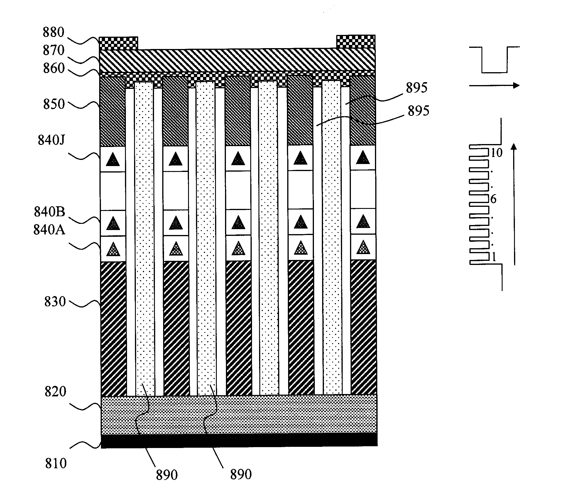
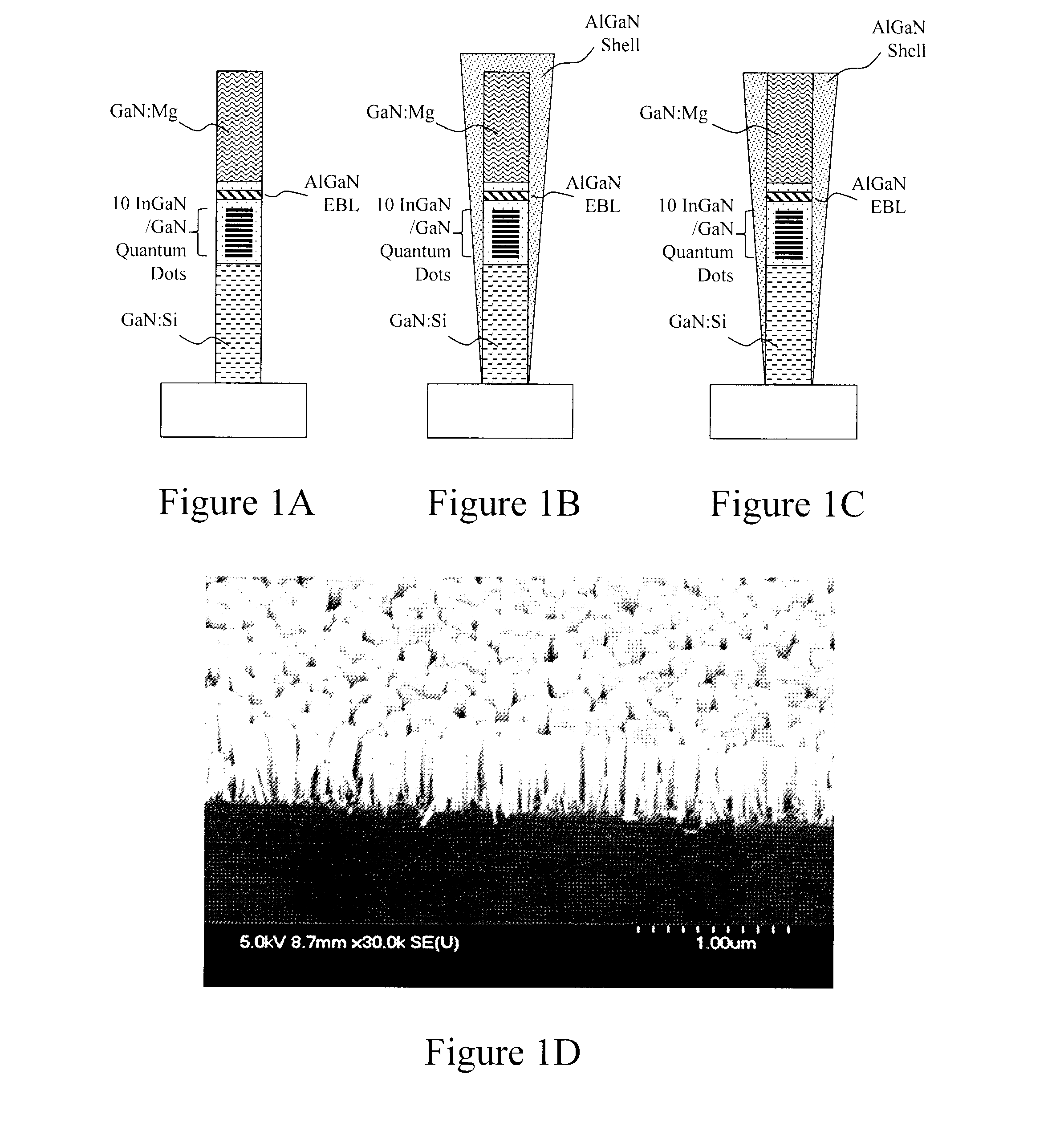
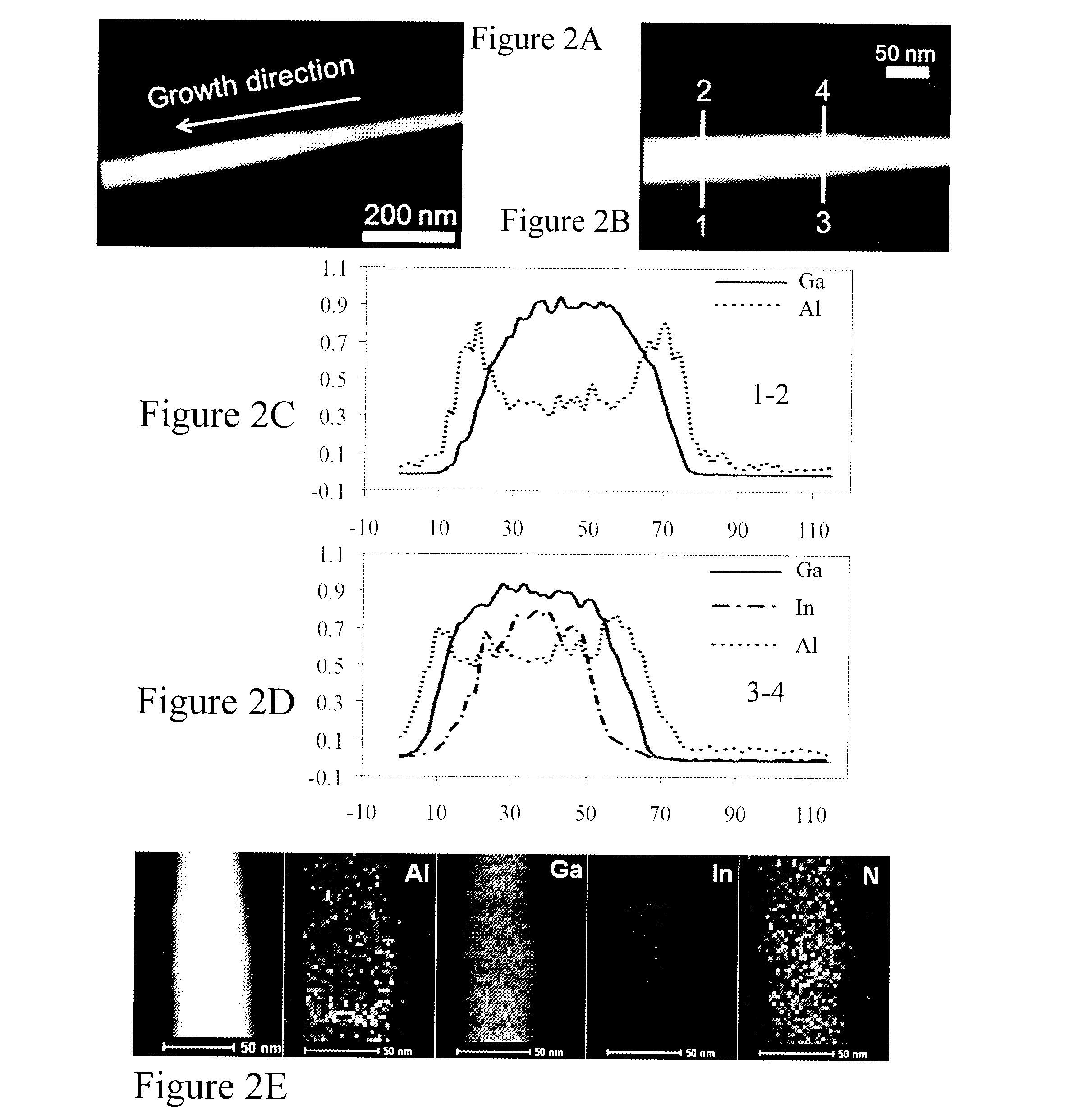
[0052]Within the experiments reported below for devices the inventors have exploited vertically aligned InGaN / GaN dot-in-a-wire LED heterostructures grown on Si(111) substrates by radio-frequency plasma-assisted molecular beam epitaxy under nitrogen-rich conditions. Descriptions of such structures can be found for example within US Patent...
PUM
 Abstract
Description
Claims
Application Information
 - R&D Engineer
- R&D Manager
- IP Professional
- Industry Leading Data Capabilities
- Powerful AI technology
- Patent DNA Extraction
Browse by: Latest US Patents, China's latest patents, Technical Efficacy Thesaurus, Application Domain, Technology Topic, Popular Technical Reports.
© 2024 PatSnap. All rights reserved.Legal|Privacy policy|Modern Slavery Act Transparency Statement|Sitemap|About US| Contact US: help@patsnap.com