Single crystal acoustic resonator and bulk acoustic wave filter

a single crystal acoustic resonator and filter technology, applied in the field of single crystal acoustic resonators and bulk acoustic wave filters, can solve the problems of high acoustic velocity in the resonator, and achieve the effects of simple and cost effective, cost-effective, and advantage in physical material properties

Active Publication Date: 2016-01-28
AKOUSTIS INC
View PDF0 Cites 151 Cited by
  • Summary
  • Abstract
  • Description
  • Claims
  • Application Information

AI Technical Summary

Benefits of technology

[0009]One or more benefits are achieved over pre-existing techniques using the invention. In particular, the invention enables a cost-effective resonator device for communications applications with a 30% advantage in physical material properties. In a specific embodiment, the present device can be manufactured in a relatively simple and cost effective manner. Depending upon the embodiment, the present apparatus and method can be manufactured using conventional materials and / or methods according to one of ordinary skill in the art. The present device uses aluminum, gallium and nitrogen containing material that is single crystalline. Depending upon the embodiment, one or more of these benefits may be achieved. Of course, there can be other variations, modifications, and alternatives.

Problems solved by technology

The substrate structure has a substrate member comprising a lattice constant chosen to closely match the lattice constant of single crystal piezoelectric material resulting in high acoustic velocity in the resonator.

Method used


Image

  • Single crystal acoustic resonator and bulk acoustic wave filter
  • Single crystal acoustic resonator and bulk acoustic wave filter
  • Single crystal acoustic resonator and bulk acoustic wave filter

Examples


Embodiment Construction

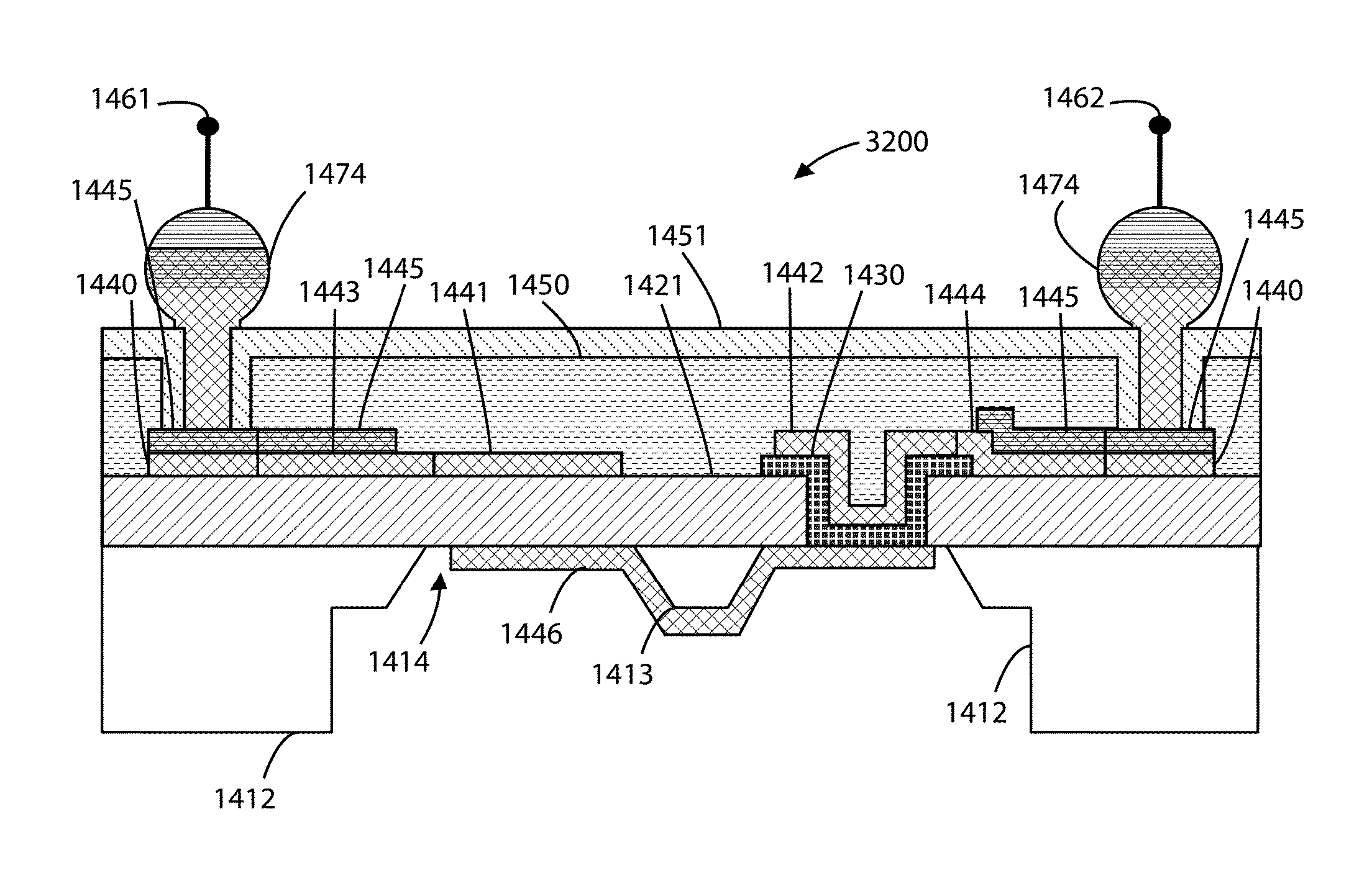
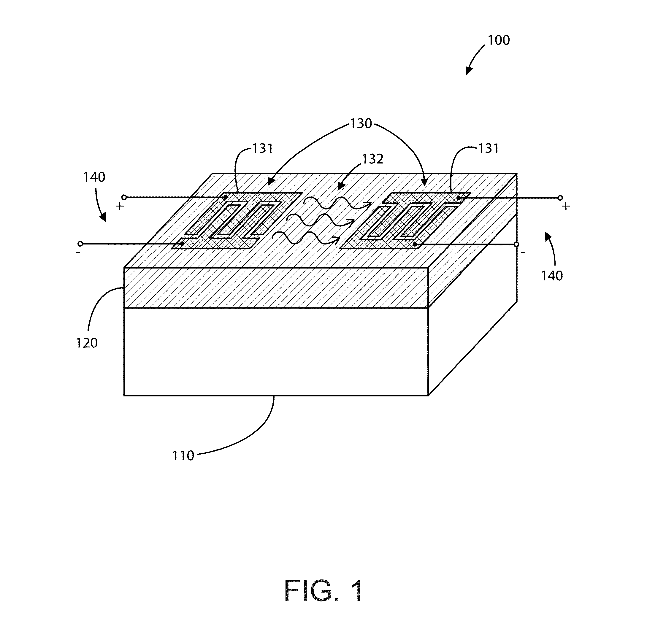
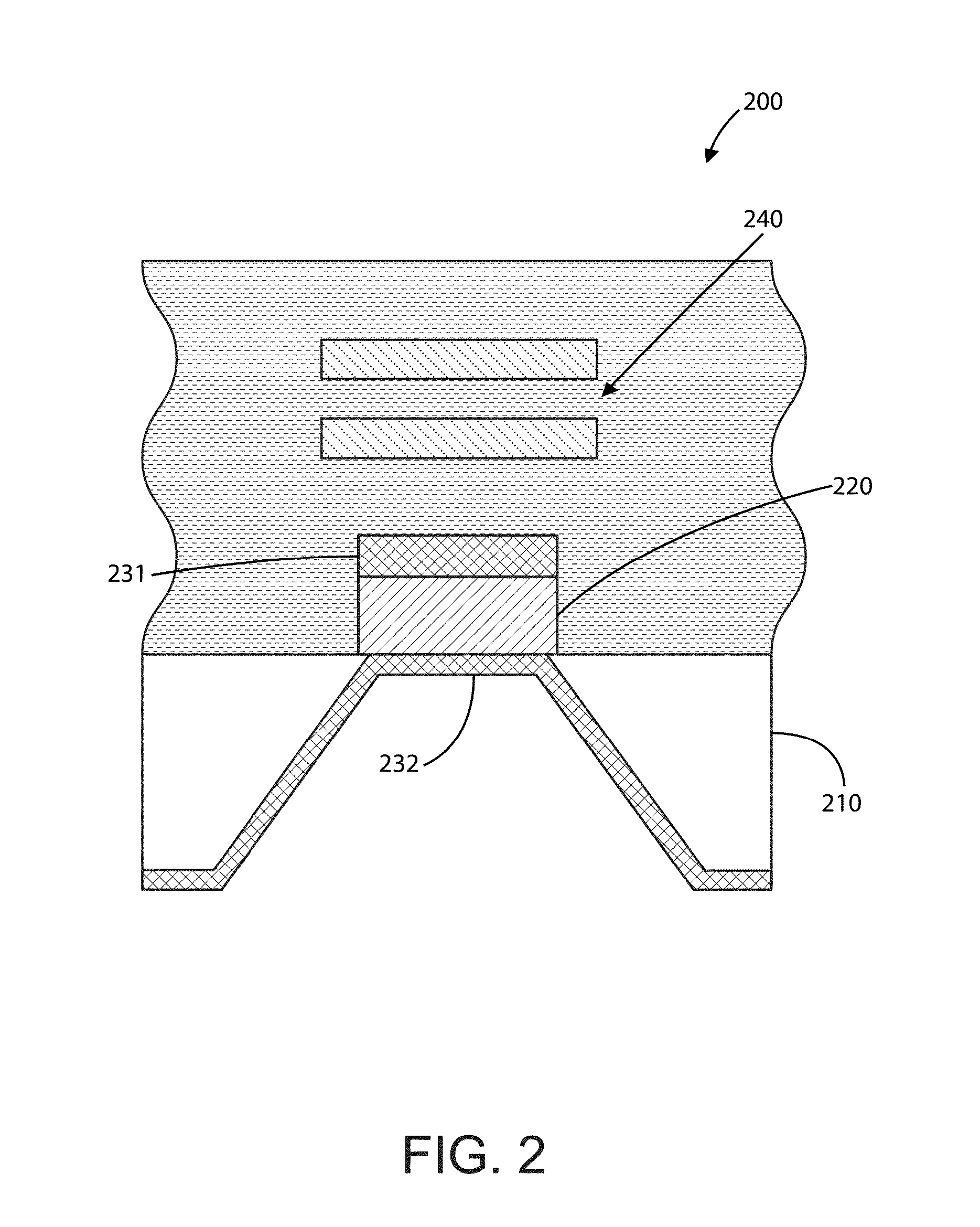
[0034]According to the present invention, techniques generally related to electronic devices are provided. More particularly, the present invention provides techniques related to a single crystal acoustic resonator. Merely by way of example, the invention has been applied to a resonator device for a communication device, mobile device, computing device, among others.

[0035]As additional background, the number of bands supported by smartphones is estimated to grow by 7-fold compared to conventional techniques. As a result, more bands mean high selectivity filter performance is becoming a differentiator in the RF front end of smartphones. Unfortunately, conventional techniques have severe limitations.

[0036]That is, conventional filter technology is based upon amorphous materials and whose electromechanical coupling efficiency is poor (only 7.5% for non-lead containing materials) leading to nearly half the transmit power dissipated in high selectivity filters. In addition, single crysta...


PUM


Abstract

A method of wafer scale packaging acoustic resonator devices and an apparatus therefor. The method including providing a partially completed semiconductor substrate comprising a plurality of single crystal acoustic resonator devices provided on a silicon and carbide bearing material, each having a first electrode member, a second electrode member, and an overlying passivation material. At least one of the devices to be configured with an external connection, a repassivation material overlying the passivation material, an under metal material overlying the repassivation material. Copper pillar interconnect structures are then configured overlying the electrode members, and solder bump structures are form overlying the copper pillar interconnect structures.

Description

CROSS-REFERENCES TO RELATED APPLICATIONS[0001]The present application is a continuation-in-part application of the following filed patent application, commonly owned: U.S. patent application Ser. No. 14 / 341,314, (Attorney Docket No.: A969RO-000400US) titled “WAFER SCALE PACKAGING”, filed Jul. 25, 2014. The present application incorporates by reference, for all purposes, the following filed patent applications, all commonly owned: U.S. patent application Ser. No. 14 / 298,057, (Attorney Docket No. A969RO-000100US) titled “RESONANCE CIRCUIT WITH A SINGLE CRYSTAL CAPACITOR DIELECTRIC MATERIAL”, filed Jun. 6, 2014, U.S. patent application Ser. No. 14 / 298,076, (Attorney Docket No. A969RO-000200US) titled “METHOD OF MANUFACTURE FOR SINGLE CRYSTAL CAPACITOR DIELECTRIC FOR A RESONANCE CIRCUIT”, filed Jun. 6, 2014, U.S. patent application Ser. No. 14 / 298,100, (Attorney Docket No. A969RO-000300US) titled “INTEGRATED CIRCUIT CONFIGURED WITH TWO OR MORE SINGLE CRYSTAL ACOUSTIC RESONATOR DEVICES”,...

Claims


Application Information

Patent Timeline
Patent Type & Authority Applications(United States)
IPC IPC(8): H01L41/18H03H9/17H01L41/29H01L41/316H03H9/205
CPCH03H9/171H01L41/316H03H9/205H01L41/18H01L41/29H03H9/02031H03H9/0523H03H9/174H03H2003/023H03H3/02H01L2224/13082H01L2224/13147H01L2224/13101H01L2224/16225
Inventor SHEALY, JEFFREY, B.
Owner AKOUSTIS INC
Why Eureka
Try Eureka