Eureka AIR delivers breakthrough ideas for toughest innovation challenges, trusted by R&D personnel around the world.

Charge-transporting thin film

a thin film and charge-transporting technology, applied in the direction of non-metal conductors, conductors, electrolytic capacitors, etc., can solve the problems of not exploiting the properties common organic materials, affecting the use of organic materials, and generally involving problems, so as to achieve small variations in properties, small variations in resistance, and small variations over time

Active Publication Date: 2016-03-10
MERCK PATENT GMBH
View PDF5 Cites 10 Cited by
  • Summary
  • Abstract
  • Description
  • Claims
  • Application Information

AI Technical Summary

Benefits of technology

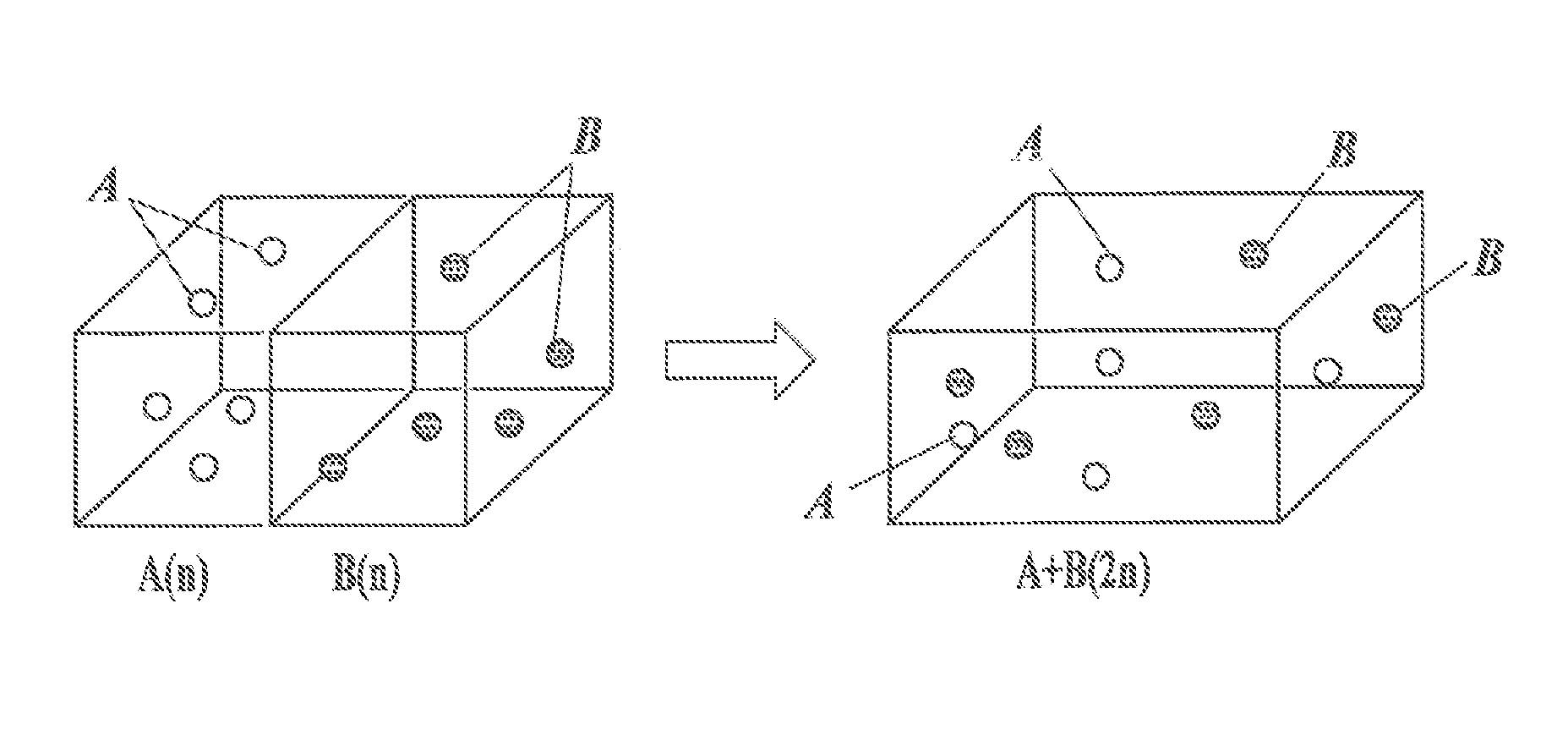
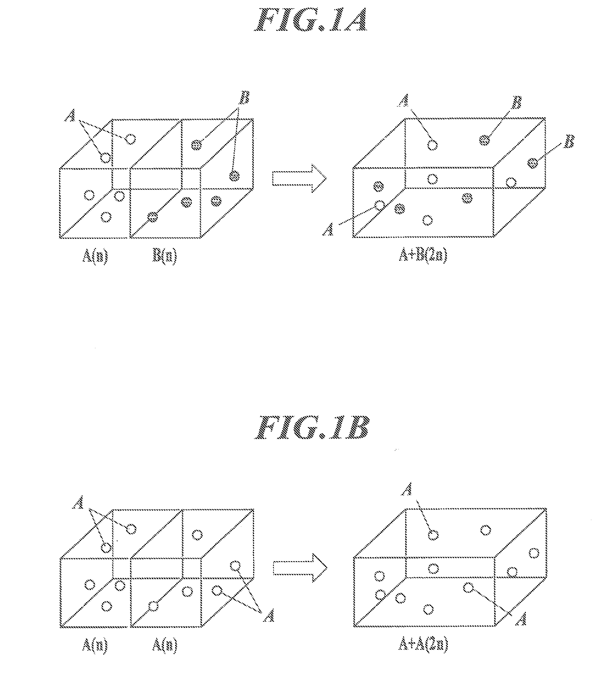
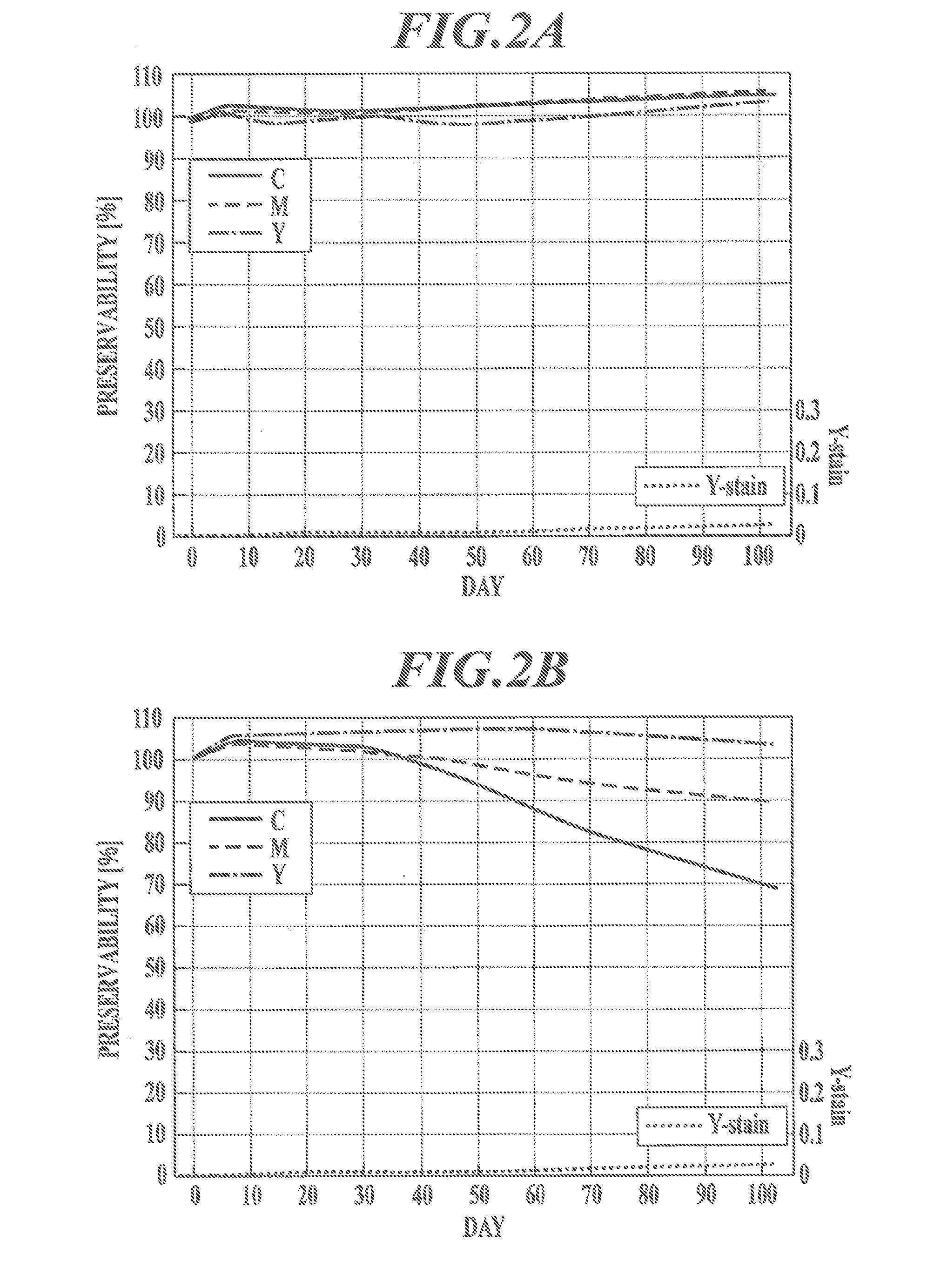
The present invention provides a charge-transporting thin film that has small variations in properties and resistance over time during application of current. The thin film also has a secondary effect of small variations over time and stable luminescent properties. The invention effectively exploits entropic effects of functional organic compounds with chiral elements. Overall, the invention employs a combination of functional organic compounds in a way that maximizes the intended effects.

Problems solved by technology

Industrial components made of organic materials, particularly electronic devices and electronic components to which a high electric field is applied, generally involve problems due to the nature of the organic materials used therein, i.e. thermal degradation and electrochemical deterioration that are characteristics of organic substances.
The use of such organic materials unfortunately fails to exploit properties common organic materials have, such as solubility, flexibility, chemical reactivity, and compatibility with other materials.
Such characteristics of organic materials are inappropriate for future industrial applications.
In the actual circumstances, the way of molecular design has not been very active in view of the coexistence of multiple molecules.
Unfortunately, even such techniques fail to achieve sufficient stability required for charge-transporting thin films, where a current is generally applied for a long time, under conditions expected in the market.

Method used


Image

  • Charge-transporting thin film
  • Charge-transporting thin film
  • Charge-transporting thin film

Examples


example 1

[0231]In the Example below, the charge-transporting thin film is a luminous layer, and the functional organic compounds are a luminescent dopant and a host compound.

>

[0232]Indium tin oxide (ITO) with a thickness of 100 nm was deposited on a glass substrate with dimensions of 100 mm by 100 mm by 1.1 mm (NA 45 manufactured by NH Technoglass Corporation) and was patterned into an anode. A transparent support substrate provided with the transparent ITO electrode was ultrasonically cleaned in isopropyl alcohol, was dried in a dry nitrogen stream, and then was cleaned in a UV ozone environment for five minutes.

[0233]A solution of 70% poly(3,4-ethylene dioxythiophene)-polyethylenesulfonate (hereinafter, referred to as PEDOT / PSS; Baytron P Al 4083 available from Bayer) in pure water was applied by spin coating on the transparent support substrate at 3000 rpm for 30 seconds. The coating film was dried at 200° C. for one hour. A hole injection layer with a thickness of 20 nm was thereby forme...

example 2

[0250]Another Example will now be described. In this example, the charge-transporting thin film is a luminous layer, and the functional organic compounds are a luminescent dopant and a host compound, as in Example 1.

>

[0251]Indium tin oxide (ITO) with a thickness of 100 nm was deposited on a glass substrate with dimensions of 100 mm by 100 mm by 1.1 mm (NA 45 manufactured by NH Technoglass Corporation) and was patterned into an anode. A transparent support substrate provided with the transparent ITO electrode was ultrasonically cleaned in isopropyl alcohol, was dried in a dry nitrogen stream, and then was cleaned in a UV ozone environment for five minutes.

[0252]A solution of 70% poly(3,4-ethylene dioxythiophene)-polyethylenesulfonate (PEDOT / PSS; Baytron P Al 4083 available from Bayer) in pure water was applied by spin coating on the transparent support substrate at 3000 rpm for 30 seconds. The coating film was dried at 200° C. for one hour. A first hole transport layer with a thickne...

example 3

[0261]Another Example will now be described. In this example, the charge-transporting thin film is a luminous layer, and the functional organic compounds are a luminescent dopant and a host compound.

>

[0262]Indium tin oxide (ITO) with a thickness of 100 nm was deposited on a glass substrate with dimensions of 100 mm by 100 mm by 1.1 mm (NA 45 manufactured by NH Technoglass Corporation) and was patterned into an anode. A transparent support substrate provided with the transparent ITO electrode was ultrasonically cleaned in isopropyl alcohol, was dried in a dry nitrogen stream, and then was cleaned in a UV ozone environment for five minutes.

[0263]The transparent support substrate was fixed to a substrate holder in a commercially available vacuum vapor deposition system, and 200 mg of TPD (N,N′-bis(3-methylphenyl)-N,N′-diphenyl-(1,1′-biphenyl)-4,4′-diamine) was placed onto a molybdenum resistive heating boat, 200 mg of CBP was placed onto another molybdenum resistive heating boat, 200 m...


PUM

PropertyMeasurementUnit
boiling pointaaaaaaaaaa
charge-transportingaaaaaaaaaa
electric fieldaaaaaaaaaa

Abstract

This invention addresses the problem of providing a charge-transporting thin film with small variations in properties due to disturbance and small variations in resistance over time during application of current. The invention further provides a charge-transporting thin film with a secondary effect of small variations over time and stable luminescent properties. The charge-transporting thin film of the present invention contains one or more types of functional organic compounds having chiral elements, and is characterized in that the total of the number of chiral elements per molecule in each type of the functional organic compounds summed over all types of the functional organic compounds is four or more.

Description

TECHNICAL FIELD[0001]The present invention relates to a charge-transporting thin film which has high stability.BACKGROUND ART[0002]Electronic devices to which an electric field is applied, such as organic electroluminescent elements (hereinafter, also referred to as “organic EL elements”), solar cells, and organic transistors, generally include charge-transporting thin films containing organic materials capable of transporting charge carriers (generic terms including electrons and holes) during application of electric fields. Various properties are required for functional organic materials contained in charge-transporting thin films, and such functional organic materials have been extensively developed in recent years.[0003]Industrial components made of organic materials, particularly electronic devices and electronic components to which a high electric field is applied, generally involve problems due to the nature of the organic materials used therein, i.e. thermal degradation and ...

Claims


Application Information

Patent Timeline
Patent Type & Authority Applications(United States)
IPC IPC(8): H01B1/12H10K99/00
CPCH01B1/121Y02E10/542Y02E10/549H01G9/2059C09K11/06H10K85/215H10K85/654H10K85/657H10K85/6572H10K85/6574H10K85/342H10K30/30H10K50/11H10K2101/10H10K30/50H10K85/611
Inventor KITA, HIROSHITANAKA, TATSUOKATAKURA, RIE
Owner MERCK PATENT GMBH
Why Eureka
Eureka Blog
Learn More