Nano-Structured Porous Thermoelectric Generators

a porous, nano-structure technology, applied in the manufacture/treatment of thermoelectric devices, non-metal conductors, conductors, etc., can solve the problems of high material cost, high production cost, and use of rare elements, and achieve safe and economical methods for nano-sizing silicon, high seebeck coefficient, and high work capability

Inactive Publication Date: 2016-03-10
MOSSEY CREEK TECH
View PDF9 Cites 18 Cited by
  • Summary
  • Abstract
  • Description
  • Claims
  • Application Information

AI Technical Summary

Benefits of technology

[0020]Silicon has a high Seebeck Coefficient, a high capability to work at a range of temperatures, and the ability to be tailored as a semiconductor. U.S. Pat. No. 6,638,491 teaches a safe and economical method for nano-sizing silicon safely and economically. What is needed is a silicon-based material with a low thermal conductivity.
[0023]In various example embodiments, methods and processes according to the present general inventive concept involve processing suitable silicon precursors into nano-sized grains, essentially equiaxed, which can be formed into large net shape simple or complex thick shapes and sintered into structures containing these nano structured morphologies while containing dopants, for instance boron, that provide high electrical conductivity and a high Seebeck Coefficient in such a way as to preserve high carrier concentrations and long carrier lifetime. An element for success is protecting the silicon surfaces before and during sintering from any oxidation as a small amount of oxidation in these very small grain boundaries can cause very large increases in electrical resistivity.
[0033]In some example embodiments of the present general inventive concept, a doped silicon-based thermoelectric material includes milled silicon grain particles having a median particle size of less than 3,000 nanometers, said milled silicon particles being substantially equiaxed, and a dopant mixed with milled silicon particles to form a doped silicon-containing material, said dopant reducing the thermal conductivity of the doped silicon-containing material compared to the milled silicon grain particles, said doped silicon-containing material being sintered in the absence of oxidants to form a doped silicon-based thermoelectric material.

Problems solved by technology

Many contemporary thermoelectrics present various disadvantages, including, in some instances, high material costs, high costs of production, difficulty of manufacture, the use of rare elements, the use of potentially carcinogenic or toxic substances, and limited formability.
Successful exploitation will need to combine brittle material engineering practices as TEMats, as a material class, are very brittle (i.e., low fracture toughness).
Lastly, from a perspective of size, a larger TEMat component or “leg” will promote the ability to achieve a larger DT (presuming it does not mechanically fail); this is an important issue for achieving cold temperatures too.
Incumbent technologies offer little hope of making low cost thick structures able to operate at high temperatures with high unaided DT and attractive power factors.
Traditional and new approaches to making thermoelectric generators (TEGs) are all flawed by fundamental and seemingly intractable challenges, such as high cost, high CTE, limited to thin planer structures, low S, low electrical conductivity, low mechanical strength, or use of rare and costly materials, or combinations thereof.
Many of those same issues limit the ability to achieve colder temperatures with thermoelectric coolers (TECs).
Also, thermoelectric materials, as a material class, are very brittle.
Unfortunately, these structures are expensive and cannot be practically made in the thick cross sections required to maintain a large unaided or largely unaided ΔT.
But they only address a “bulk” material.

Method used


Image

  • Nano-Structured Porous Thermoelectric Generators
  • Nano-Structured Porous Thermoelectric Generators
  • Nano-Structured Porous Thermoelectric Generators

Examples


Embodiment Construction

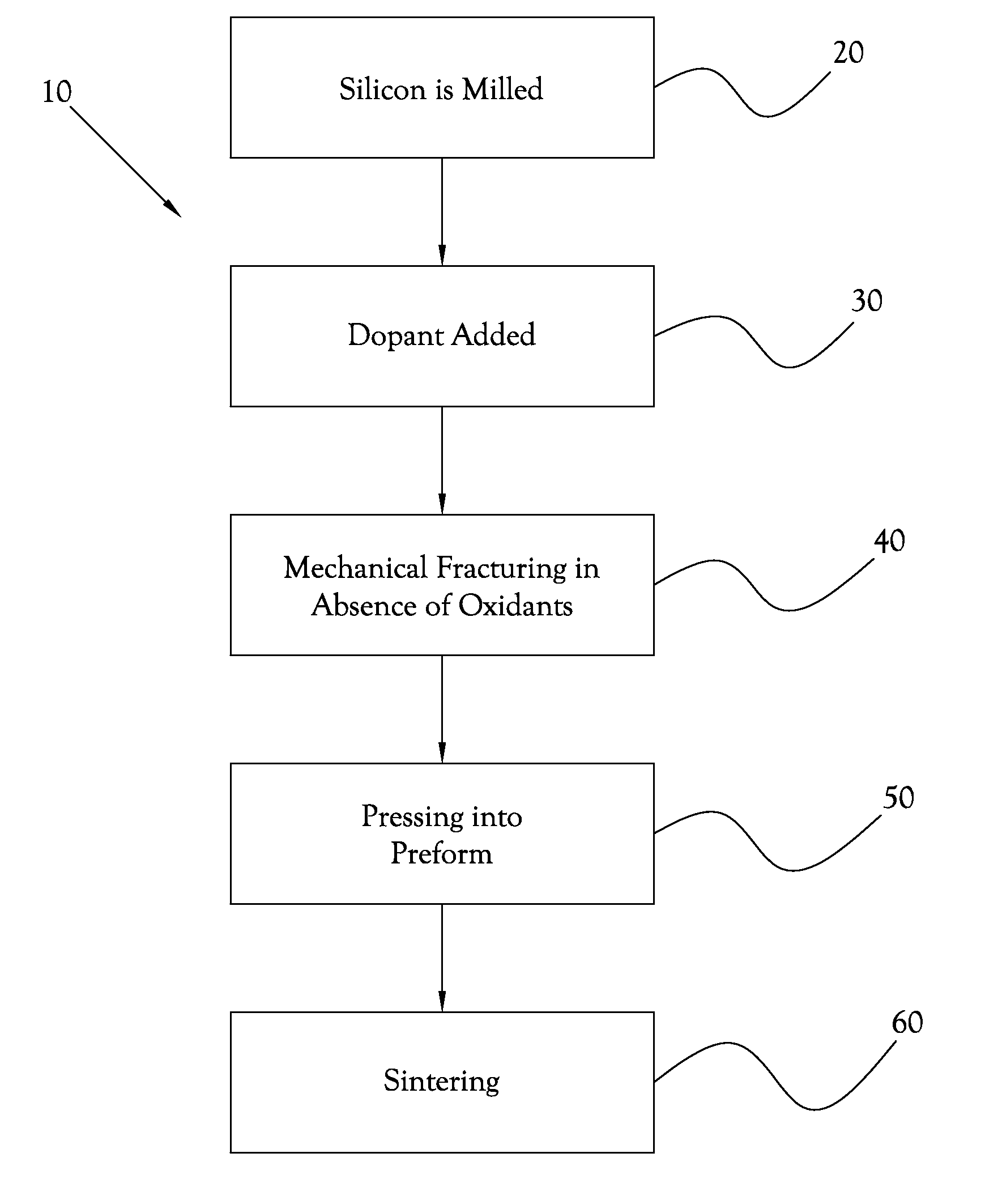
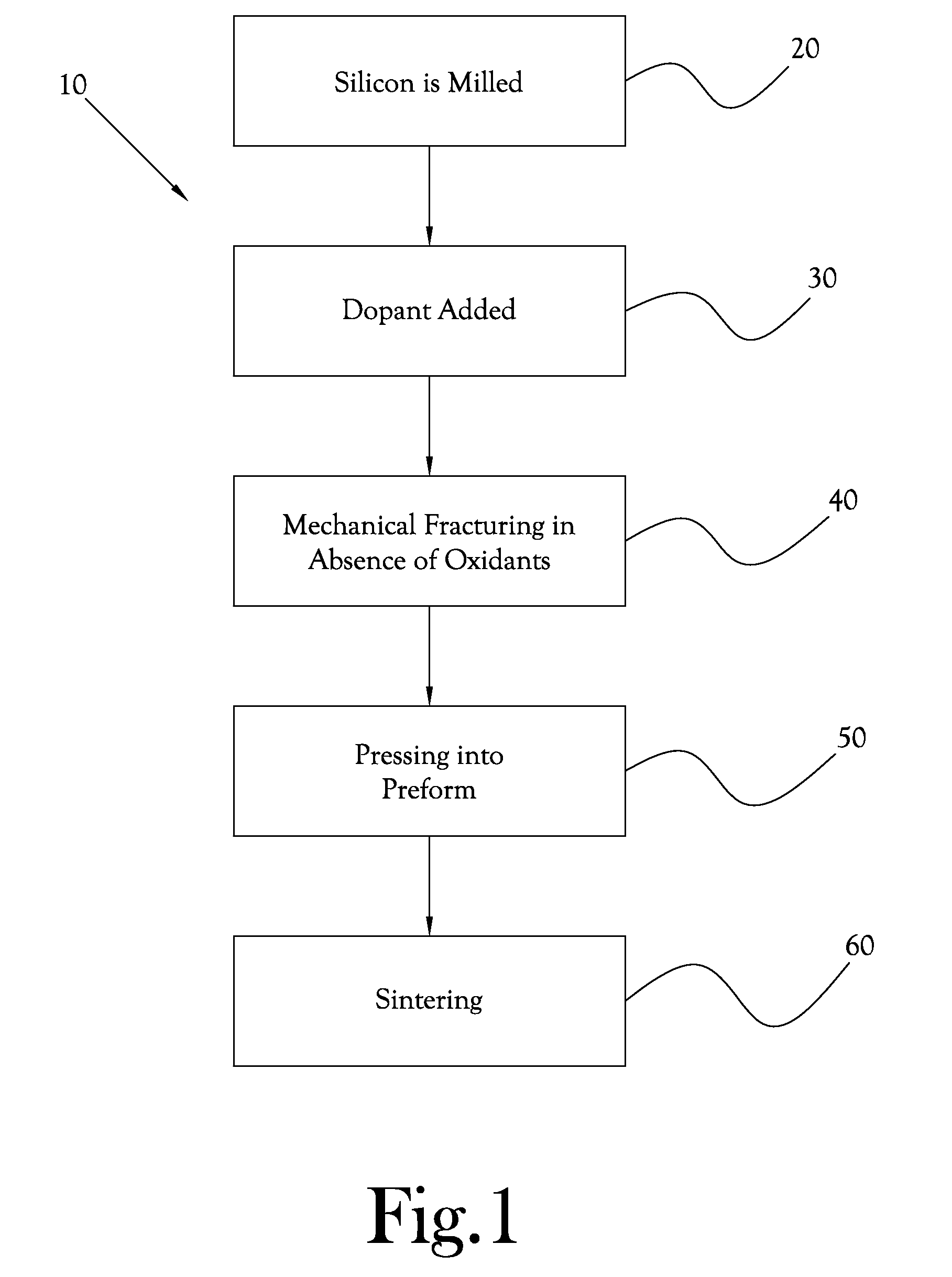
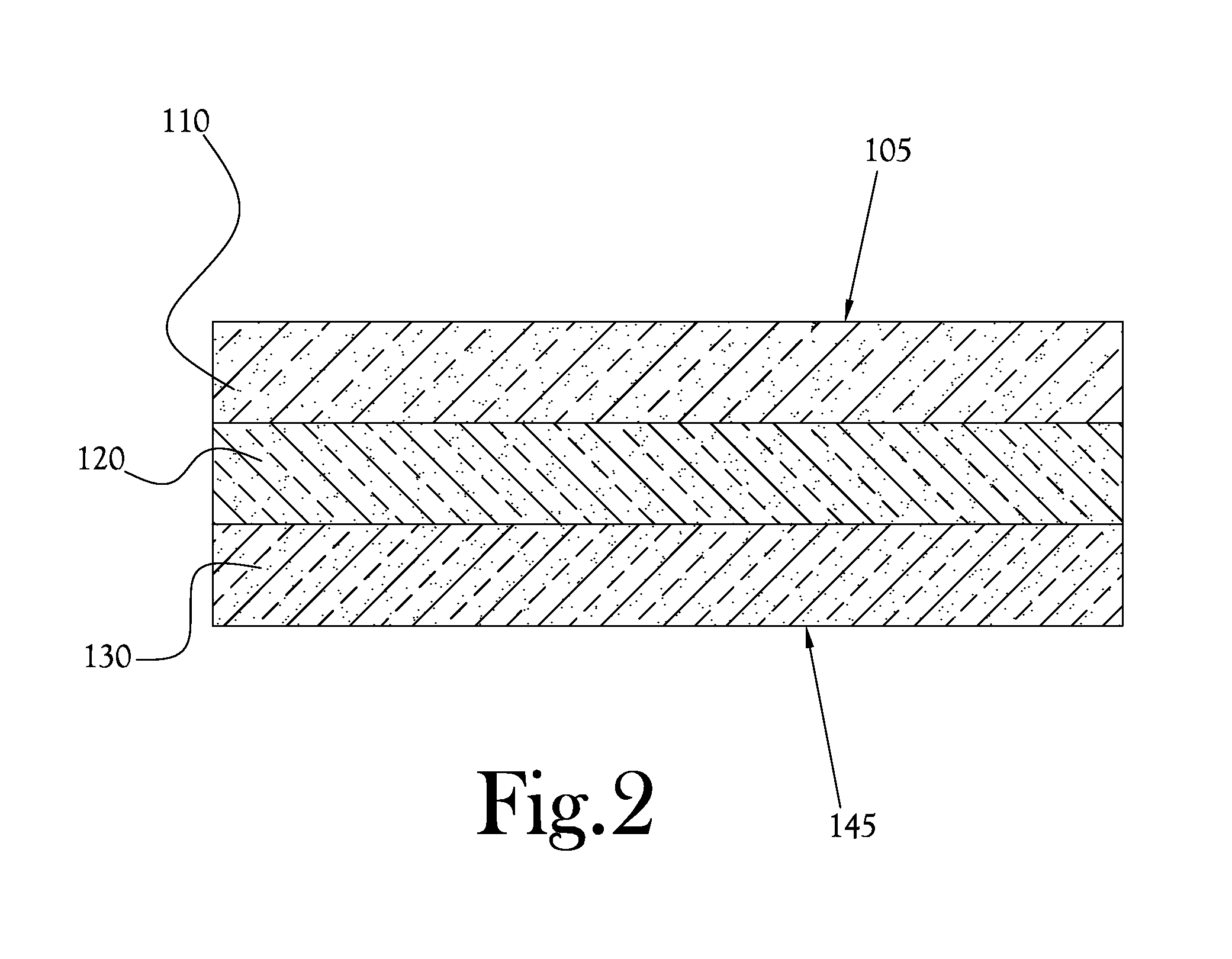
[0053]Disclosed herein are methods and processes to fabricate thermoelectric materials and more particularly to methods and processes to fabricate doped silicon-based semiconductive materials to use as thermoelectrics in the production of electricity from recovered waste heat. In some example embodiments, the present invention comprises a thermoelectric material that incorporates a silicon-based semiconductor material.

[0054]Also disclosed herein are methods and processes that encompass the use a high-purity, properly-doped, nanostructured, porous silicon milled to a particle size less than a few microns, and sinter into a thick structure that will achieve a very high efficiency converting heat to electricity.

[0055]In various example embodiments of the present general inventive concept, fabrication of effective silicon-based thermoelectric devices involves: doping for high electrical conductivity for both P and N type by doping from column III and column V of the periodic chart respe...


PUM

PropertyMeasurementUnit
median sizeaaaaaaaaaa
temperatureaaaaaaaaaa

Abstract

Methods and processes to fabricate thermoelectric materials and more particularly to methods and processes to fabricate nano-sized doped silicon-based semiconductive materials to use as thermoelectrics in the production of electricity from recovered waste heat. Substantially oxidant-free and doped silicon particulates are fractured and sintered to form a porous nano-sized silicon-based thermoelectric material.

Description

CROSS-REFERENCE TO RELATED APPLICATIONS[0001]This application claims the benefit of U.S. Provisional Patent Application No. 62 / 046,434, filed Sep. 5, 2014, the content of which is incorporated by reference herein in its entirety.STATEMENT REGARDING FEDERALLY SPONSORED RESEARCH OR DEVELOPMENT[0002]Not ApplicableBACKGROUND OF THE INVENTION[0003]1. Field of Invention[0004]The present general inventive concept relates to the preparation and use of thermoelectric materials and more particularly to methods and processes to fabricate doped thermoelectric generators, especially doped silicon-based thermoelectric generators.[0005]2. Description of the Related Art[0006]Semiconductive materials that exhibit the Seebeck and Peltier effects in the presence of a temperature gradient are useful for the production of electricity from waste heat. Semiconductive materials which move heat from one side to the other when presented with an electrical charge from one side to the other are useful for cool...

Claims


Application Information

Patent Timeline
Patent Type & Authority Applications(United States)
IPC IPC(8): H01L35/16H01L35/20H01L35/22H01L35/34
CPCH01L35/16H01L35/34H01L35/22H01L35/20H10N10/855H10N10/852H10N10/01C04B35/6261C04B35/64C04B35/65H10N10/854
Inventor CARBERRY, JOHN
Owner MOSSEY CREEK TECH
Why Eureka
Try Eureka