

Method of manufacturing transparent substrate provided with cured film, photosensitive resin composition, photosensitive element, and electrical component
a technology of transparent substrate and resin composition, which is applied in the direction of photosensitive materials, instruments, photomechanical equipment, etc., can solve the problems of increased production cost, limitation of base materials, and inability to meet the requirements of alumina-based substrates, and achieve the effect of sufficient anti-corrosion properties, enhanced conductivity and desired film properties
- Summary
- Abstract
- Description
- Claims
- Application Information
AI Technical Summary
Benefits of technology
Problems solved by technology
Method used
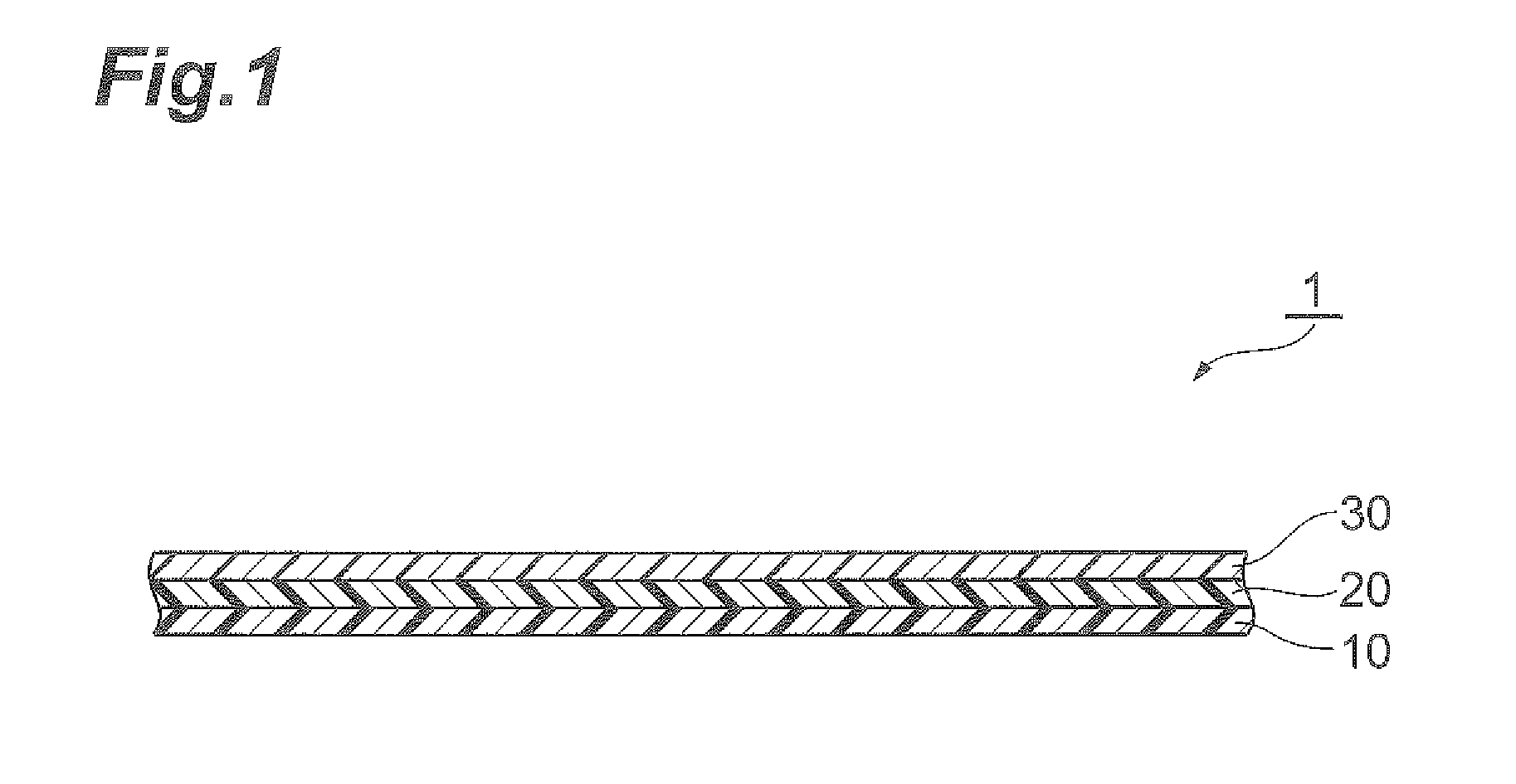
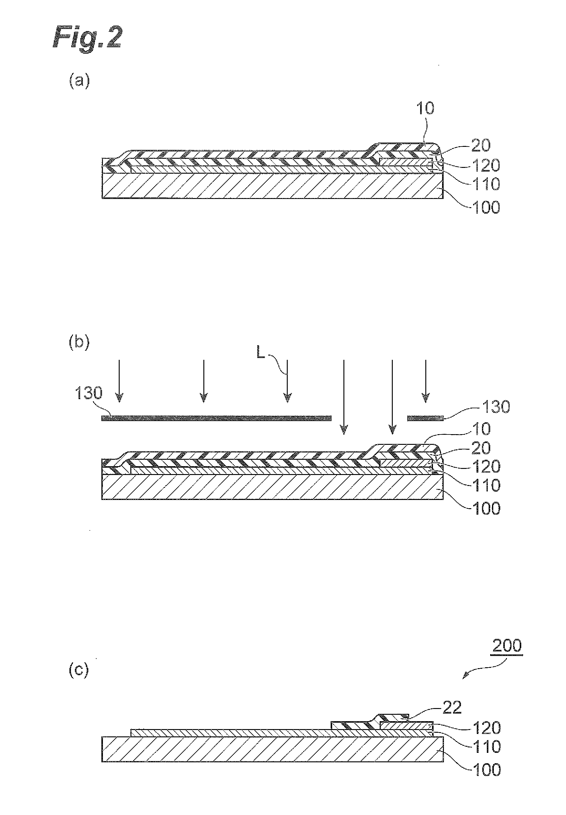
Image

Examples
example 1
Preparation of Photosensitive Resin Composition Solution (V-1) for Forming Cured Film
[0207]The materials shown in Table 2 were mixed with a stirrer for 15 minutes to prepare Photosensitive resin composition solution (V-1) for forming a cured film.
TABLE 2Amount of compounding amountComponentMaterials(parts by mass)(A)(A1)60(B)T-1420 (T)40(C)OXE011.7OthersB60300.4Methyl ethyl ketone50
[0208][Preparation of Photosensitive Element (E-1) for Forming Cured Film]
[0209]A poly(ethylene terephthalate) film having a thickness of 50 μm was used as a support film, Photosensitive resin composition solution (V-1) was uniformly applied onto the support film with a comma coater, and the solvent was removed by drying with a 100° C. hot air convection dryer for 3 minutes to form a photosensitive layer (photosensitive resin composition layer) composed of a photosensitive resin composition. The thickness of the obtained photosensitive layer was 5 μm.
[0210]Next, a polyethylene film having a thickness of 2...
examples 2 to 4
[0236]Photosensitive elements were prepared in the same manner as in Example 1 except that photosensitive resin composition solutions shown in Table 3 (units for the numeric values in Table are parts by mass) were used, and were subjected to the saline water spray test, the mandrel test, and the determination of degree of moisture permeation. As shown in Table 3, in Examples 1 to 4, good results were obtained in the evaluation of resistance against saline water, the mandrel test, and the determination of degree of moisture permeation.
TABLE 3ItemsExampleComparative ExampleNames of materials12341234Binder polymerA160———60606060A2—60——————A360————A460————PhotopolymerizableT-1420 (T)40404040————compoundOtherA-TMMT————40———photopolymerizableRP-1040—————40——compoundsBPE-500——————40—4G———————40PhotopolymerizationOXE011.71.71.71.71.71.71.71.7initiatorOthersAW5000.10.10.10.10.10.10.10.1SH-300.070.070.070.070.070.070.070.07MEK5050505050505050Resistance against saline waterABBBCCDDCrack resist...
PUM
| Property | Measurement | Unit |
|---|---|---|
| thickness | aaaaa | aaaaa |
| wavelength band | aaaaa | aaaaa |
| light transmittance | aaaaa | aaaaa |
Abstract
Description
Claims
Application Information