Nitride semiconductor light-emitting device

a semiconductor light-emitting and semiconductor technology, applied in semiconductor lasers, semiconductor devices, electrical devices, etc., can solve problems such as affecting device design, affecting device performance, and affecting device design, so as to improve the efficiency of current injection and improve the efficiency of positive holes in the active layer

Active Publication Date: 2016-05-26
MEIJO UNIVERSITY
View PDF0 Cites 29 Cited by
  • Summary
  • Abstract
  • Description
  • Claims
  • Application Information

AI Technical Summary

Benefits of technology

[0008]The active layer is interposed between the first and second composition-graded layers in this nitride semiconductor light-emitting device. Furthermore, each one of the first and second composition-graded layers is composition-graded so that an Al composition value thereof is rendered smaller as each one of the first and second composition-graded layers comes close to a side where a sum of spontaneous polarization and piezoelectric polarization is negative. Accordingly, of the polarization fixed charges in the first and second composition-graded layers, negative polarization fixed charges are averaged to be distributed in a thicknesswis

Problems solved by technology

Accordingly, a nitride semiconductor having a multilayer structure, such as a nitride semiconductor light-emitting device could lead to occurrence of unnecessary polarization fixed charge o

Method used


Image

  • Nitride semiconductor light-emitting device
  • Nitride semiconductor light-emitting device
  • Nitride semiconductor light-emitting device

Examples


first embodiment

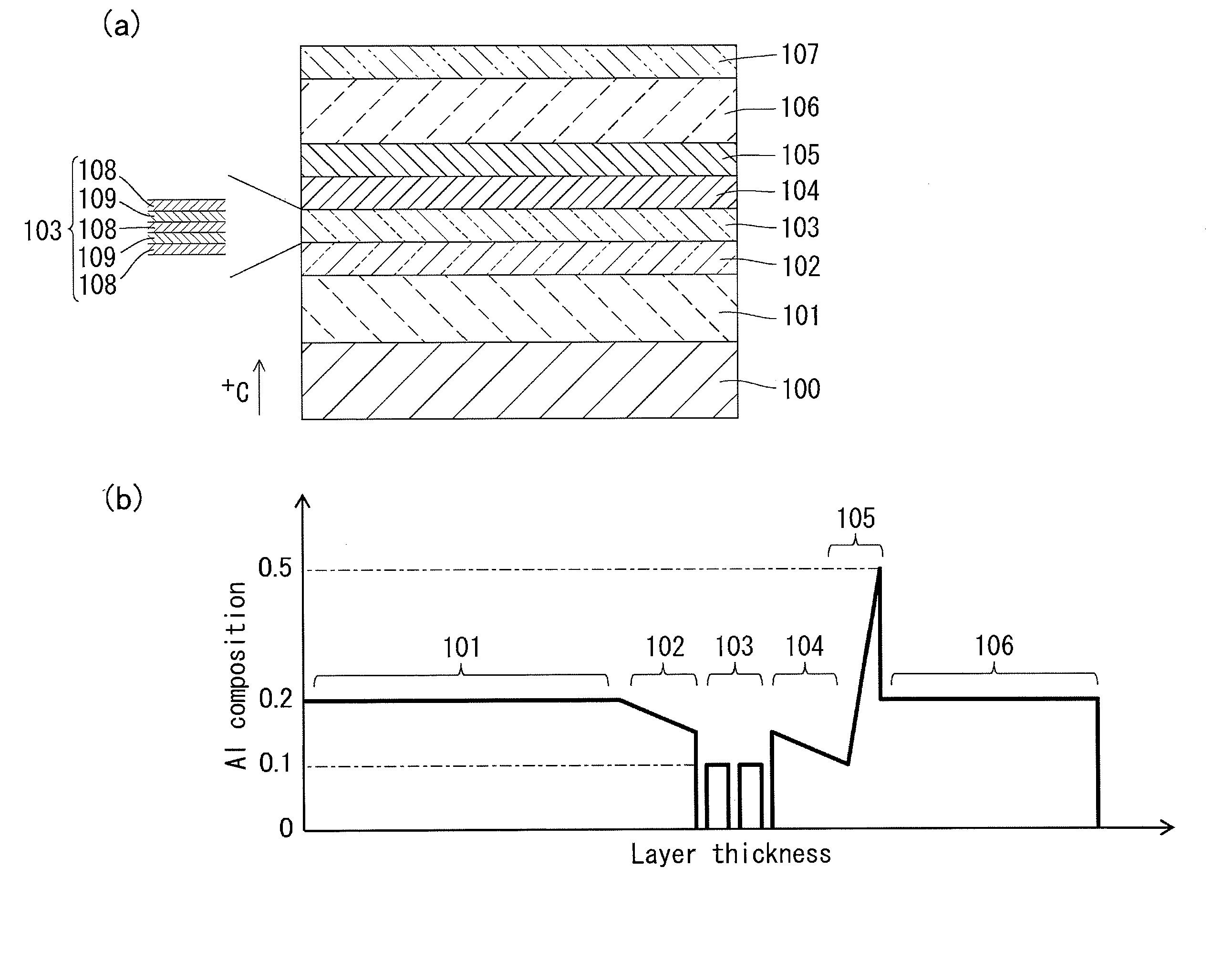
[0025]FIGS. 1(a) and 1(b) show a sectional structure of an ultraviolet (UV) laser diode according to the first embodiment and an Al composition profile of layers of the laser diode, respectively. The UV laser diode includes a triple quantum well active layer (an active layer) 103 further including GaN quantum well layers 108 and Al0.1Ga0.9N barrier layers 109, and first and second AlGaN composition-graded layers (first and second composition-graded layers) 102 and 104 at both sides of the triple quantum well active layer 103 in a stacking direction respectively. More specifically, the triple quantum well active layer 103 is interposed between the first and second composition-graded AlGaN layers 102 and 104.

[0026]The UV laser diode is formed by stacking, on a c-plane GaN oriented in a +c-axis direction or an AIN polar substrate 100, an n-type Al0.2Ga0.8N clad layer 101, the first composition-graded AlGaN layer 102, the GaN triple quantum well active layer 103, the second composition-...


PUM


Abstract

An object is to improve a positive hole injection efficiency into an active layer in a nitride semiconductor light-emitting device. The nitride semiconductor light-emitting device is formed by stacking nitride semiconductor crystals each of which contains Al and has a polar or semipolar surface either serving as a growth face. The device includes an active layer (103), and first and second composition-graded layers (102, 104). The active layer (103) is interposed between the first and second composition-graded layers (102, 104). Each one of the first and second composition-graded layers is composition-graded so that an Al composition value is rendered smaller as each one of the first and second composition-graded layers (102, 104) comes close to a side where a sum of spontaneous polarization and piezoelectric polarization is negative.

Description

TECHNICAL FIELD[0001]The present invention relates to a nitride semiconductor light-emitting device.BACKGROUND ART[0002]Nitride semiconductors as represented by nitride gallium (GaN) have a difficulty in obtaining a high concentration of positive holes, and the positive hole mobility is smaller than the electron mobility in the nitride semiconductors. Accordingly, a positive hole injection efficiency into an active layer is required to be improved in order that a current injection type high-efficient light emitting device may be realized. To deal with this problem, there is known a method of obtaining a high positive hole concentration by attracting positive holes using polarization fixed charge which is generated on a crystal interface by spontaneous polarization or piezoelectric polarization each as a physical property inherent in a nitride semiconductor material. However, polarization is caused while positive and negative fixed charges are paired with electrical neutrality being ...

Claims


Application Information

Patent Timeline
IPC IPC(8): H01L33/14H01L33/18H01L33/32H01L33/06
CPCH01L33/145H01L33/32H01L33/18H01L33/06H01S5/3054H01S5/3409H01S5/34333H01L33/02H01S5/320225H01S5/3213
Inventor TAKEUCHI, TETSUYAIWAYA, MOTOAKIAKASAKI, ISAMU
Owner MEIJO UNIVERSITY
Why Eureka
Try Eureka