Gas sensor, method for manufacturing gas sensor, and method for detecting gas concentration

a technology of gas sensor and manufacturing method, which is applied in the direction of liquid/fluent solid measurement, material resistance, metallic material coating process, etc., can solve the problems of unstable semiconductor layer at high temperatures, and low durability of sensors, and achieve high temperature stability, good durability, and good characteristics

Inactive Publication Date: 2016-06-09
MURATA MFG CO LTD
View PDF1 Cites 4 Cited by
  • Summary
  • Abstract
  • Description
  • Claims
  • Application Information

AI Technical Summary

Benefits of technology

[0023]This makes it easy for gas molecules to physically adsorb onto the interface between the n-type and p-type semiconductor layers, allowing changes in resistance associated with electrolysis to be used to detect the concentration of the gas.
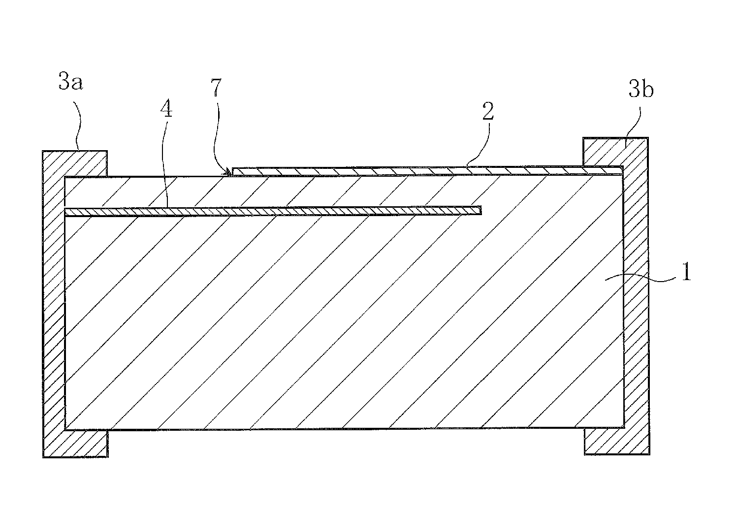
[0024]A method according to the present invention for manufacturing a gas sensor is characterized by including a shaped-article production step including producing a shaped article made mainly of a solid solution of NiO and ZnO, a firing step including firing the shaped article to obtain a p-type semiconductor layer as a sintered body, and a sputtering step including forming an n-type semiconductor layer on the surface of the p-type semiconductor layer by sputtering using a target material made mainly of at least one of ZnO and TiO2. This method, utilizing sputtering to form an n-type semiconductor layer on a p-type semiconductor layer which is a sintered body, provides an easy way to obtain a gas sensor that offers good characteristics and high-temperature stability and excellent durability.
[0025]A method according to the present invention for manufacturing a gas sensor is characterized by including a shaped-article production step including producing a shaped article made mainly of a solid solution of NiO and ZnO, a sheet-shaped member production step including producing a sheet-shap...

Problems solved by technology

In Non-patent Document 1 and Patent Document 1, however, the following problems are encountered because the p-type semiconductor material is CuO or NiO.
That is, when the p-type semiconductor material is a CuO-based material, prolonged operation can cause decomposition of part of CuO and diffusion of Cu ions over the surface of the n-type semiconductor layer.
In ...

Method used


Image

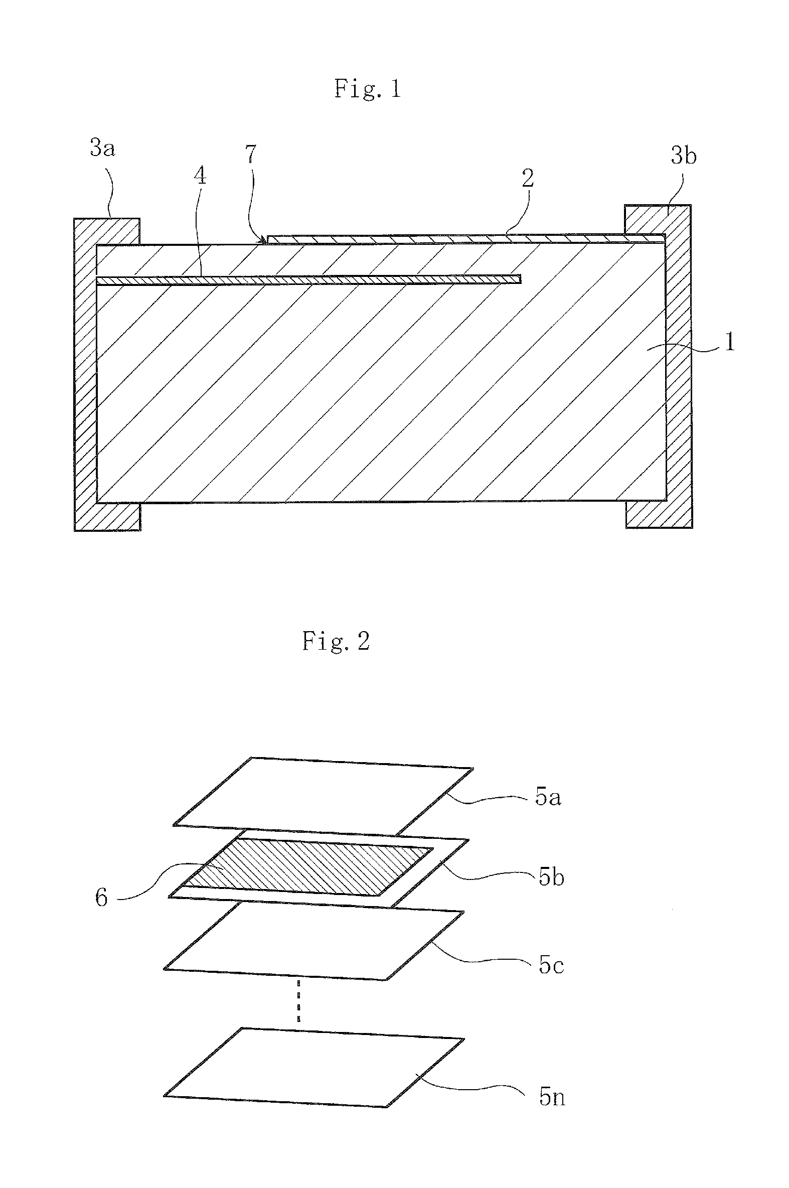
  • Gas sensor, method for manufacturing gas sensor, and method for detecting gas concentration
  • Gas sensor, method for manufacturing gas sensor, and method for detecting gas concentration
  • Gas sensor, method for manufacturing gas sensor, and method for detecting gas concentration

Examples


example 1

Sample Number 1

[0077][Production of a ZnO Sintered Body]

[0078]ZnO to serve as main component and Al2O3 as a dopant were weighed out to make the respective proportions in mol % 99.99 mol % and 0.01 mol %. These apportioned materials were mixed and milled together with purified water in a ball mill using PSZ beads as milling medium, yielding a mixture in the form of slurry with an average particle diameter of 0.5 μm or less. This slurry mixture was dried by dehydration and granulated to a particle diameter of approximately 50 μm. The resulting particles were calcined at a temperature of 1200° C. for 2 hours, yielding a calcined powder.

[0079]The thus obtained calcined powder was mixed and milled again together with purified water in a ball mill using PSZ beads as milling medium, yielding slurry of milled matter with an average particle diameter of 0.5 μm. This slurry of milled matter was dried by dehydration and then mixed together with an organic solvent and a dispersant. A binder and...

example 2

Production of Samples

Sample Numbers 21 to 25

[0122]Samples of sample numbers 21 to 25 were produced using the same method and procedure as for sample number 1, except that the molar ratio of Ni to Zn, or Ni / Zn, in preparing the (Ni, Zn)O green sheets was matched to the proportions in Table 2.

Sample Number 26

[0123]A sample of sample number 26 was produced using the same method and procedure as for sample number 1, except that the inner electrode material was LaNiO3.

[0124]The production of LaNiO3 was as follows.

[0125]That is, NiO and La2O3 powders were weighed out to a molar ratio of 2:1. These apportioned materials were mixed and milled together with purified water in a ball mill using PSZ beads as milling medium, yielding a mixture in the form of slurry. This slurry mixture was dried by dehydration and granulated to a particle diameter of approximately 50 μm. The resulting particles were calcined at a temperature of 1200° C. for 2 hours, yielding a calcined powder. The calcined powde...


PUM

PropertyMeasurementUnit
Percent by moleaaaaaaaaaa
Concentrationaaaaaaaaaa
Molar ratioaaaaaaaaaa

Abstract

A humidity sensor that includes a p-type semiconductor layer and an n-type semiconductor layer on the p-type semiconductor layer. The p-type semiconductor layer is a sintered body made mainly of a solid solution of NiO and ZnO, and the n-type semiconductor layer is made mainly of at least one of ZnO and TiO2. The p-type semiconductor layer has a molar ratio of Ni to Zn, or Ni/Zn, of 6/4 or more and 8/2 or less. The n-type semiconductor layer is produced using sputtering or through the firing of a multilayer structure composed of a green multilayer body to be made into the p-type semiconductor layer and a green sheet thereon to be made into the n-type semiconductor layer.

Description

CROSS REFERENCE TO RELATED APPLICATIONS[0001]The present application is a continuation of International application No. PCT / JP2014 / 065541, filed Jun. 12, 2014, which claims priority to Japanese Patent Application No. 2013-179530, filed Aug. 30, 2013, the entire contents of each of which are incorporated herein by reference.FIELD OF THE INVENTION[0002]The present invention relates to a gas sensor, a method for manufacturing a gas sensor, and a method for detecting a gas concentration. To be more specific, the present invention relates to a pn-junction gas sensor including p-type and n-type oxide semiconductor layers joined together at a heterojunction, a method for manufacturing this gas sensor, and a method for detecting the concentration of an ambient gas using this gas sensor.BACKGROUND OF THE INVENTION[0003]There have been various forms proposed of humidity sensors, which detect the concentration of water vapor in the air, and other gas sensors.[0004]For example, Non-patent Docum...

Claims


Application Information

Patent Timeline
IPC IPC(8): G01N27/407G01N33/18
CPCG01N27/4071G01N2033/0095G01N33/18G01N27/12B32B18/00C04B35/01C04B35/453C04B35/62675C04B2235/3217C04B2235/3224C04B2235/3227C04B2235/3244C04B2235/3263C04B2235/3279C04B2235/3284C04B2235/5445C04B2235/6025C04B2237/34C04B2237/346C04B2237/68C04B2237/704C23C14/08
Inventor NAKAMURA, KAZUTAKA
Owner MURATA MFG CO LTD
Why Eureka
Try Eureka