
Wiring board with dual wiring structures integrated together and method of making the same

Inactive Publication Date: 2016-06-16
BRIDGE SEMICON
View PDF4 Cites 6 Cited by
  • Summary
  • Abstract
  • Description
  • Claims
  • Application Information

AI Technical Summary

Benefits of technology

The present invention provides a wiring board with two integrated wiring structures that allow for high routing flexibility and signal integrity. The stiffener provides mechanical support for the first wiring structure and helps to prevent warping and bending of the wiring board, improving its mechanical reliability. The two wiring structures are positioned in a through opening of the stiffener, increasing the production yield of the wiring board. The method of making the wiring board involves inserting a sacrificial carrier and the first wiring structure into the stiffener before the formation of the second wiring structure, providing a stable platform for the second wiring structure and avoiding micro-via connection failure and serious warping problem when multiple layers of wiring circuitries are needed.

Problems solved by technology

However, although the inductance of these wiring boards can be reduced, other features such as design flexibility are not addressed as they do not have adequate fan-out routing capability to meet stringent requirements for ultra-fine flip chip assembly.

Method used


Image

  • Wiring board with dual wiring structures integrated together and method of making the same
  • Wiring board with dual wiring structures integrated together and method of making the same
  • Wiring board with dual wiring structures integrated together and method of making the same

Examples


embodiment 1

[0041]FIGS. 1-17 are schematic views showing a method of making a wiring board that includes a stiffener, a first wiring structure and a second wiring structure in accordance with an embodiment of the present invention.

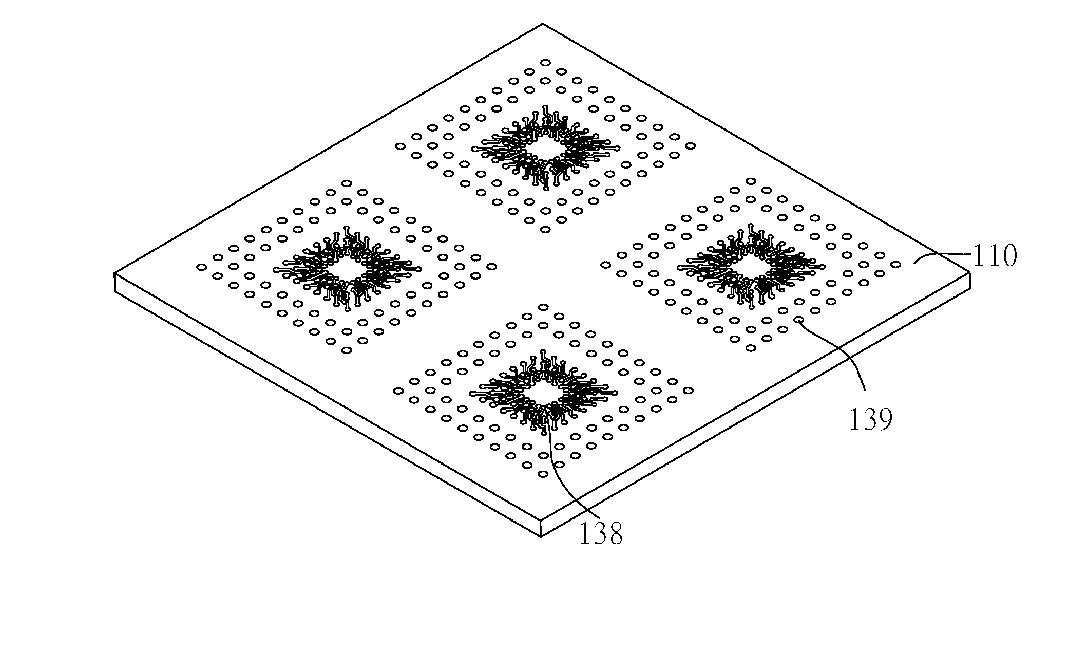
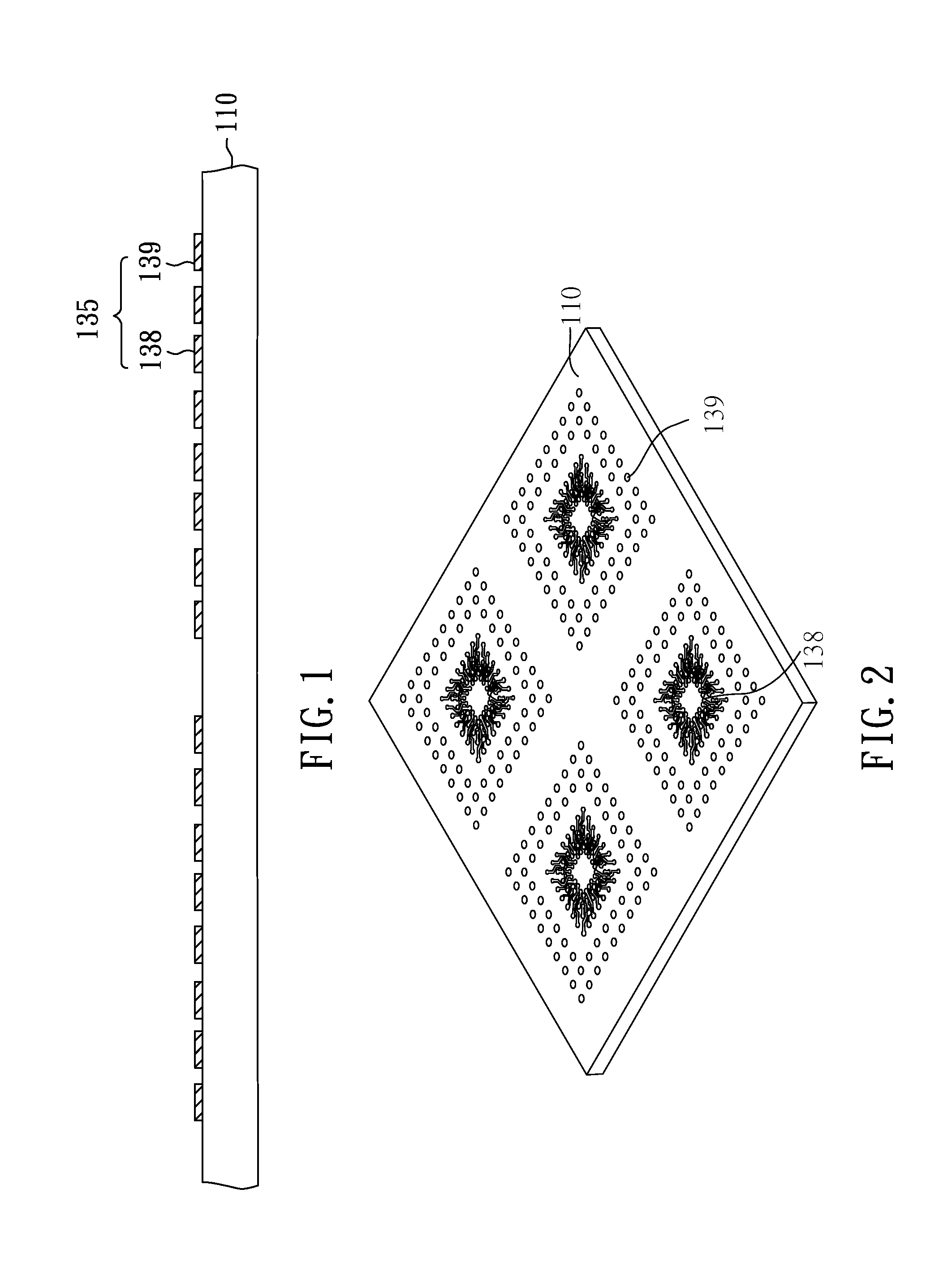
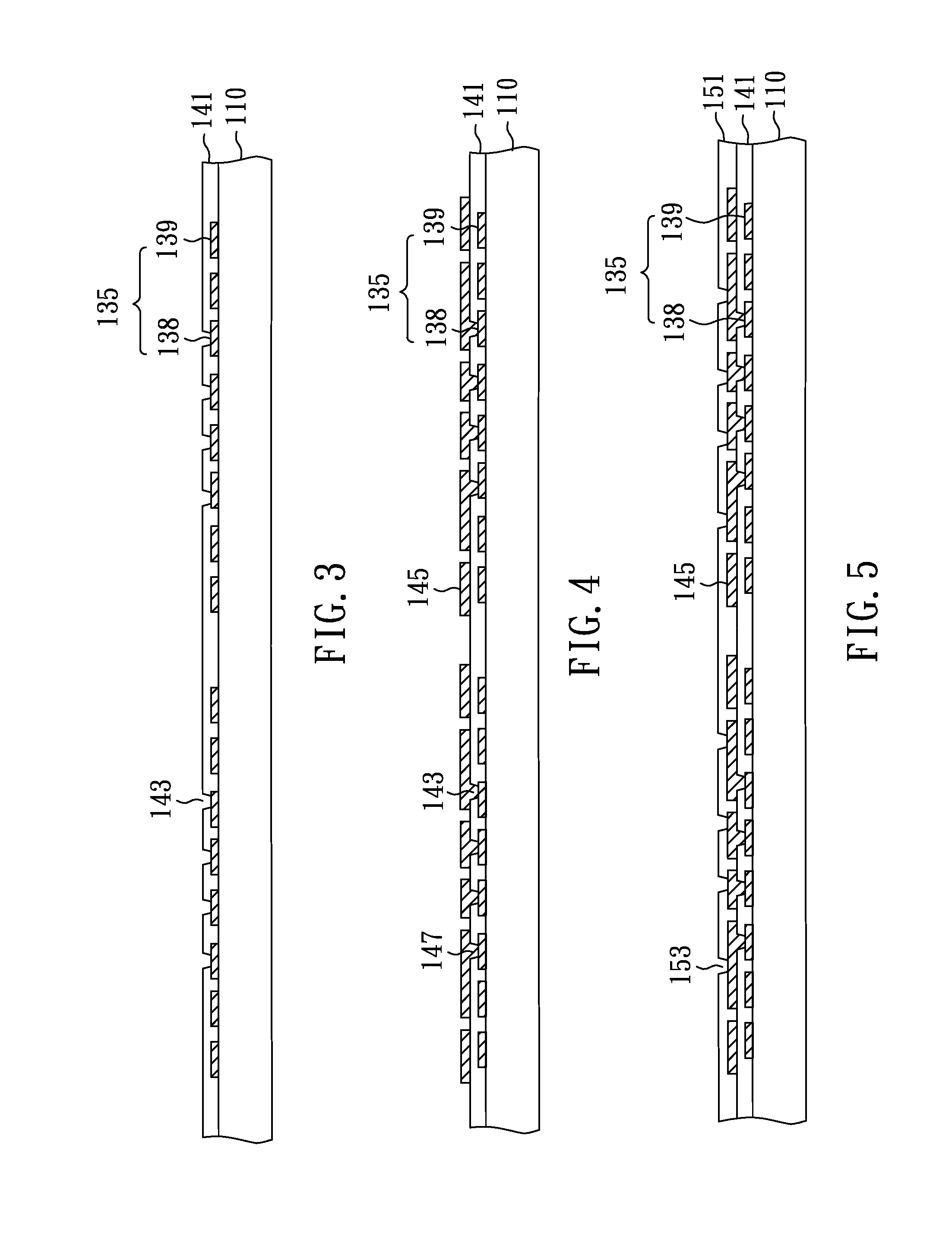
[0042]FIGS. 1 and 2 are cross-sectional and top perspective views, respectively, of the structure with routing traces 135 formed on a sacrificial carrier 110 by metal deposition and metal patterning process. In this illustration, the sacrificial carrier 110 is a single-layer structure, and the routing traces 135 include bond pads 138 and stacking pads 139. The sacrificial carrier 110 typically is made of copper, aluminum, iron, nickel, tin, stainless steel, silicon, or other metals or alloys, but any other conductive or non-conductive material also may be used. The thickness of the sacrificial carrier 110 preferably ranges from 0.1 to 2.0 mm. In this embodiment, the sacrificial carrier 110 is made of an iron-based material and has a thickness of 1.0 mm. The routing tr...

embodiment 2

[0065]FIGS. 20-28 are schematic views showing a method of making another wiring board with an anti-warping controller in accordance with another embodiment of the present invention.

[0066]For purposes of brevity, any description in Embodiment 1 above is incorporated herein insofar as the same is applicable, and the same description need not be repeated.

[0067]FIG. 20 is a cross-sectional view of the structure with a subcomponent 10 and a stiffener 20 on a third insulating layer 441 / a metal layer 44. The subcomponent 10 is similar to that illustrated in FIG. 10, except that the sacrificial carrier 110 is a double-layer structure in this embodiment. In this illustration, the third insulating layer 441 is sandwiched between the subcomponent 10 and the metal layer 44 and between the stiffener 20 and the metal layer 44, and contacts the second conductive traces 155 of the subcomponent 10 and the second surface 203 of the stiffener 20. The surface of second conductive traces 155 is substant...

embodiment 3

[0079]FIG. 30 is a cross-sectional view of yet another wiring board 300 with the second wiring structure 420 further electrically coupled to the stiffener 20 for ground connection in accordance with yet another embodiment of the present invention.

[0080]In this embodiment, the wiring board 300 is manufactured in a manner similar to that illustrated in Embodiment 2, except that the first wiring structure 120 includes no stacking pads at its first surface 101, no registration mark is formed on the second wiring structure 420, and the third conductive traces 445 of the second wiring structure 420 are further electrically coupled to the metallic stiffener 20 through additional third conductive vias 448 in direct contact with the stiffener 20.

[0081]FIG. 31 is a cross-sectional view of a semiconductor assembly with a semiconductor device 57, illustrated as a 3D-stacked chip, mounted on the wiring board 300 illustrated in FIG. 30. The semiconductor device 57 is positioned within the cavity ...


PUM

PropertyMeasurementUnit
Electrical conductoraaaaaaaaaa
Mechanical propertiesaaaaaaaaaa
Surface areaaaaaaaaaaa

Abstract

A wiring board with integrated dual wiring structures is characterized in that first and second wiring structures are positioned within and beyond a through opening of a stiffener, respectively. The mechanical robustness of the stiffener can prevent the wiring board from warping. The first wiring structure, positioned within the through opening of the stiffener, can provide primary fan-out routing, whereas the second wiring structure not only provides further fan-out wiring structure for the first wiring structure, but also mechanically binds the first wiring structure with the stiffener.

Description

CROSS REFERENCE TO RELATED APPLICATIONS[0001]This application claims the benefit of filing date of U.S. Provisional Application Ser. No. 62 / 092,196 filed Dec. 15, 2014 and the benefit of the filing date of U.S. Provisional Application Ser. No. 62 / 121,450 filed Feb. 26, 2015. The entirety of each said Provisional Applications is incorporated herein by reference.FIELD OF THE INVENTION[0002]The present invention relates to a wiring board, more particularly, to a wiring board having integrated dual wiring structures within and beyond a through opening of a stiffener, respectively, and a method of making the same.DESCRIPTION OF RELATED ART[0003]Market trends of electronic devices such as multimedia devices demand for faster and slimmer designs. One of the approaches is to interconnect semiconductor chip through a coreless substrate so that the assembled device can be thinner and signal integrity can be improved. U.S. Pat. Nos. 7,851,269, 7,902,660, 7,981,728, and 8,227,703 disclose vario...

Claims


Application Information

Patent Timeline
IPC IPC(8): H05K1/02H05K3/46H05K3/10H05K1/11
CPCH05K1/0271H05K1/0298H05K3/10H05K3/4682H05K1/115H01L23/49816H01L23/49822H01L23/49827H01L23/562H01L2224/16225H01L2224/73204H05K1/181H05K1/183H05K3/4694H01L25/065Y02P70/50
Inventor LIN, CHARLES W. C.WANG, CHIA-CHUNG
Owner BRIDGE SEMICON
Features
  • Generate Ideas
  • Intellectual Property
  • Life Sciences
  • Materials
  • Tech Scout
  • Unparalleled Data Quality
  • Higher Quality Content
  • 60% Fewer Hallucinations
Learn More