Eureka AIR delivers breakthrough ideas for toughest innovation challenges, trusted by R&D personnel around the world.

Solar cell and method for manufacturing the same

Inactive Publication Date: 2016-07-07
LG ELECTRONICS INC
View PDF12 Cites 5 Cited by
  • Summary
  • Abstract
  • Description
  • Claims
  • Application Information

AI Technical Summary

Benefits of technology

The patent text describes a method of manufacturing a solar cell using laser irradiation to simplify the process and reduce costs. The front surface field region is formed on the front surface of the semiconductor substrate without needing a separate etching process. The emitter region and back surface field region are then formed by diffusing impurities of different conductive types. The back surface field region has a shape that maximizes the area of the intrinsic semiconductor layer while maintaining contact strength and resistance. The laser is selectively irradiated onto the impurities of different conductive types to form the emitter region or back surface field region with heavy or light doping concentration, which further improves efficiency and passivation function of the solar cell.

Problems solved by technology

Therefore, an incident area of light decreases, and the efficiency of the solar cell is reduced.

Method used


Image

  • Solar cell and method for manufacturing the same
  • Solar cell and method for manufacturing the same
  • Solar cell and method for manufacturing the same

Examples


Embodiment Construction

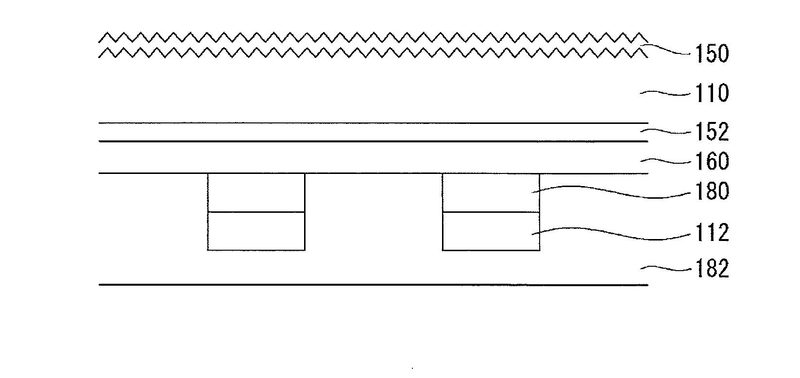
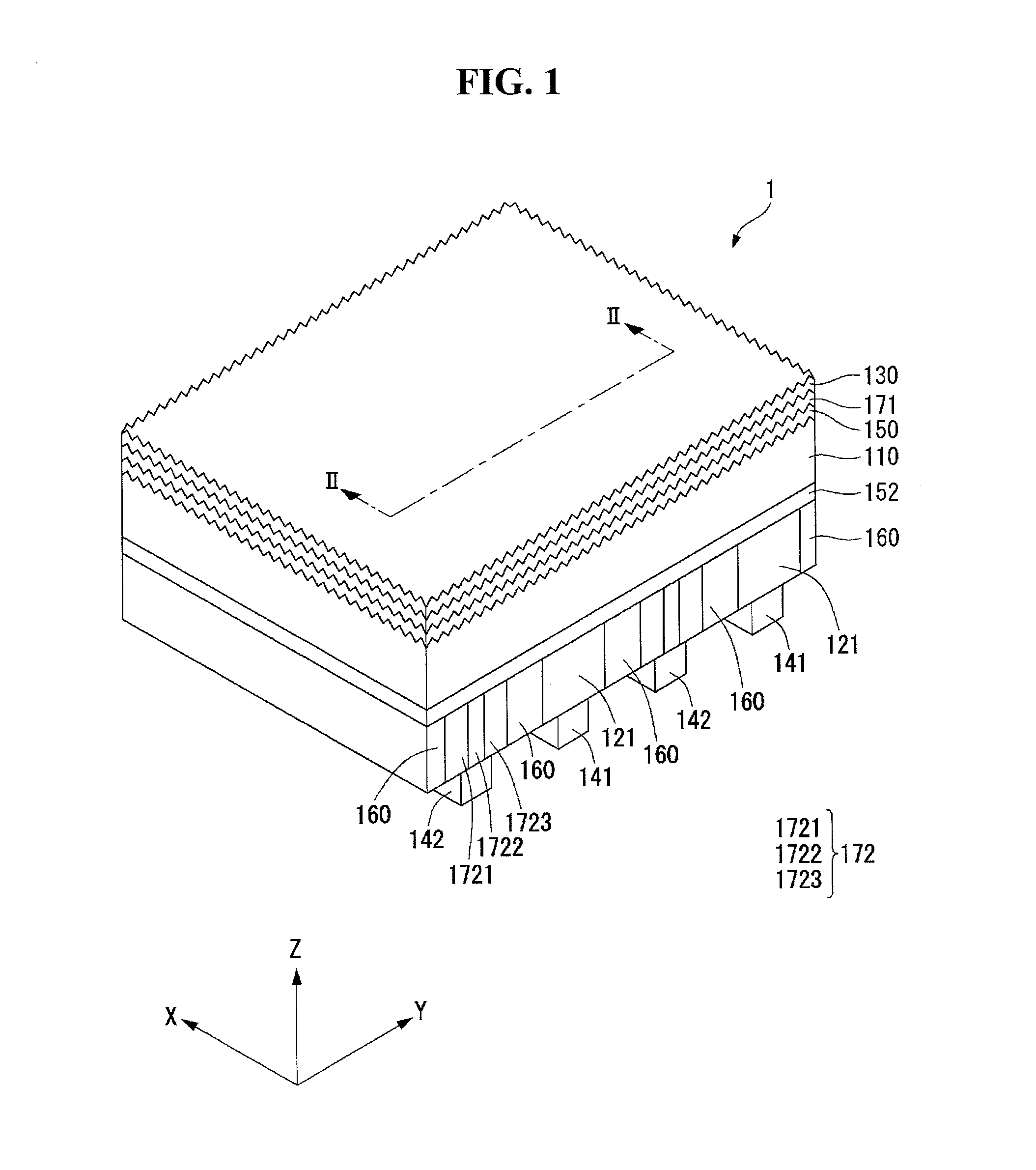
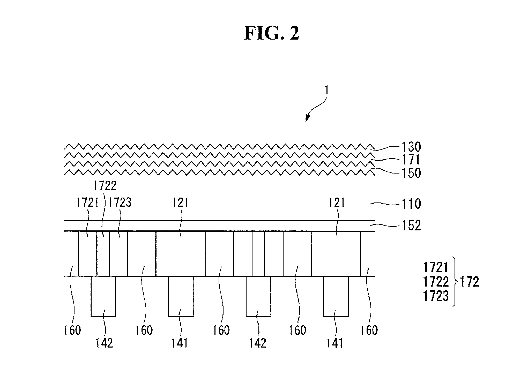
[0033]Reference will now be made in detail to embodiments of the invention, examples of which are illustrated in the accompanying drawings. This invention may, however, be embodied in many different forms and should not be construed as limited to the embodiments set forth herein. Wherever possible, the same reference numbers will be used throughout the drawings to refer to the same or like parts. It should be noted that a detailed description of the known arts will be omitted if it is determined that the detailed description of the known arts can obscure the embodiments of the invention.

[0034]In the drawings, the thickness of layers, films, panels, regions, etc., are exaggerated for clarity. It will be understood that when an element such as a layer, film, region, or substrate is referred to as being “on” another element, it can be directly on the other element or intervening elements may also be present. In contrast, when an element is referred to as being “directly on” another ele...


PUM


Abstract

A solar cell and a method for manufacturing the same are discussed. The solar cell includes a crystalline semiconductor substrate containing impurities of a first conductive type, a tunnel layer positioned on the crystalline semiconductor substrate, a semiconductor layer which is formed on the tunnel layer, has a crystallinity less than the crystalline semiconductor substrate, and includes a first doped region of a second conductive type opposite the first conductive type and a second doped region containing impurities of the first conductive type at a higher concentration than that of the crystalline semiconductor substrate, a first electrode connected to the first doped region, and a second electrode connected to the second doped region.

Description

CROSS-REFERENCE TO RELATED APPLICATION[0001]This application claims priority to and the benefit of Korean Patent Application No. 10-2015-0000916 filed in the Korean Intellectual Property Office on Jan. 5, 2015, the entire contents of which are incorporated herein by reference.BACKGROUND OF THE INVENTION[0002]1. Field of the Invention[0003]Embodiments of the invention relate to a solar cell and a method for manufacturing the same.[0004]2. Description of the Related Art[0005]Recently, as existing energy sources such as petroleum and coal are expected to be depleted, interests in alternative energy sources for replacing the existing energy sources are increasing. Hence, solar cells for generating electric energy from solar energy have been particularly spotlighted.[0006]A silicon solar cell generally includes a semiconductor substrate and an emitter region, which are formed of semiconductors of different conductive types, for example, a p-type and an n-type, and electrodes respectively...

Claims


Application Information

Patent Timeline
IPC IPC(8): H01L31/0288H01L31/077H01L31/0352H01L31/18H01L31/036
CPCH01L31/0288H01L31/18H01L31/077H01L31/035281H01L31/036H01L31/022441H01L31/0745H01L31/0747H01L31/1804H01L31/1872Y02E10/547Y02P70/50H01L31/022425H01L31/04
Inventor LEE, SEUNGJIKJI, KWANGSUNLEE, YUJINAHN, SEHWON
Owner LG ELECTRONICS INC
Why Eureka
Eureka Blog
Learn More