Electronic part mounting substrate and method for producing same

a technology for mounting substrates and electronic parts, applied in the direction of printed circuit manufacturing, sustainable manufacturing/processing, final product manufacturing, etc., can solve the problems of inability to maintain good bonding state and achieve good bonding state, excellent resistance to thermal shock, and small number of bonding defects

Active Publication Date: 2016-07-21
DOWA METALTECH CO LTD
View PDF3 Cites 11 Cited by
  • Summary
  • Abstract
  • Description
  • Claims
  • Application Information

AI Technical Summary

Benefits of technology

[0007]It is therefore an object of the present invention to eliminate the aforementioned conventional problems and to provide an electronic part mounting substrate having an excellent resistance to thermal shock, which has an electronic part bonded on a copper plate or copper-plated plate in such a good bonding state that the number of bonding defects is small and which can maintain the good bonding state if heat cycles are applied thereon, and a method for producing the same.
[0013]According to the present invention, it is possible to provide an electronic part mounting substrate having an excellent resistance to thermal shock, which has an electronic part bonded on a copper plate or copper-plated plate in such a good bonding state that the number of bonding defects is small and which can maintain the good bonding state if heat cycles are applied thereon, and a method for producing the same.

Problems solved by technology

However, in the methods disclosed in Japanese Patent Laid-Open Nos. 2011-80147, 2007-208082 and 2006-202586, if a copper plate or a copper-plated plate (an aluminum plate plated with copper) is used as a metal plate (for mounting thereon electronic parts) to bond electronic parts, such as semiconductor chips, on the metal plate with a bonding agent of a silver paste, it is not possible to bond them on such a good bonding state that the number of bonding defects is small, and it is not possible to maintain the good bonding state if heat cycles are applied thereon.

Method used


Image

  • Electronic part mounting substrate and method for producing same
  • Electronic part mounting substrate and method for producing same

Examples


example 1

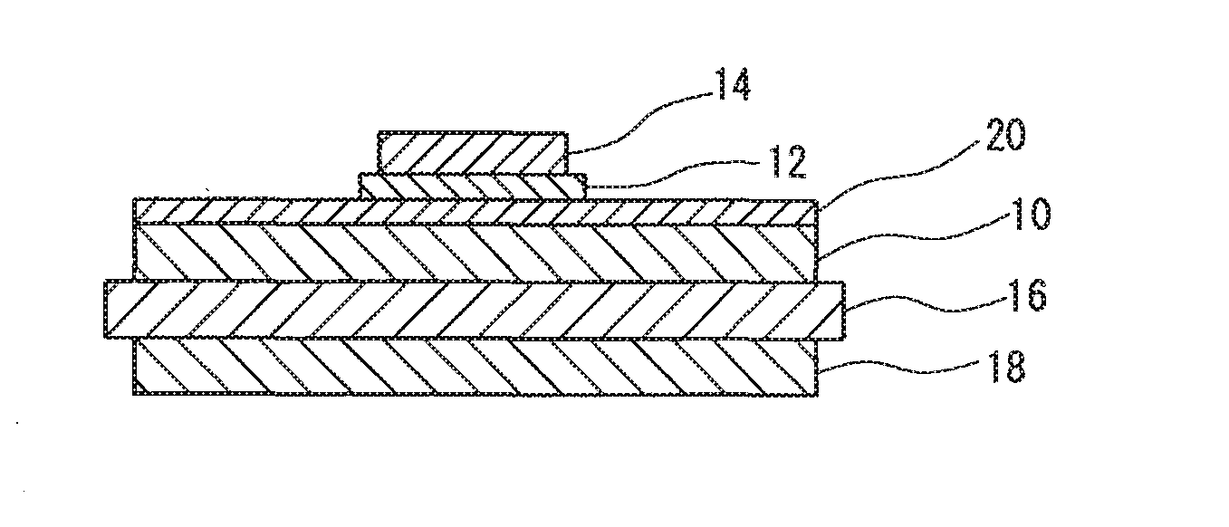
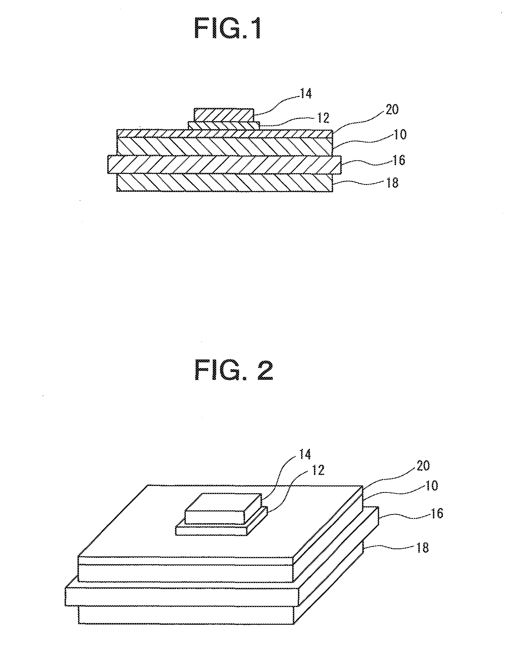
[0031]First, there were prepared a metal plate (for mounting thereon electronic parts) and metal base plate (for heat radiation) of oxygen-free copper having a size of 48 mm×57 mm×0.25 mm.

[0032]Then, one major surface of the metal plate (for mounting thereon electronic parts) was bonded to one major surface of a ceramic substrate of AlN having a size of 49 mm×58 mm×0.64 mm with an Ag—Cu brazing filler metal containing Ti as an active metal, and the metal base plate (for heat radiation) was bonded to the other surface of the ceramic substrate with the brazing filler metal, to prepare a metal / ceramic bonding substrate.

[0033]Then, the other surface of the metal plate (for mounting thereon electronic parts) of the metal / ceramic bonding substrate was surface-machined by a wet blasting apparatus (Model No. NFR-737 commercially available from MACOHO Co., Ltd.). As surface machining conditions in the wet blasting apparatus, the air pressure was 0.20 MPa, and the throughput speed was 0.3 m / m...

example 2

[0037]An electronic part mounting substrate was produced by the same method as that in Example 1, except that the metal / ceramic bonding substrate having the surface-machined metal plate (for mounting thereon electronic parts) was heated to be annealed at 370° C., for 30 minutes in an atmosphere of hydrogen gas as an atmosphere of a reducing gas. Furthermore, after the annealing was carried out, the surface roughness (arithmetic surface roughness Ra) of the (surface-machined) surface of the metal plate (for mounting thereon electronic parts) was 0.77 μm, and the Vickers hardness Hv of the (surface-machined) surface of the metal plate (for mounting thereon electronic parts) was 36.1.

[0038]With respect to the electronic part mounting substrate thus produced, the bonded portion of the Si chip to the metal plate (for mounting thereon electronic parts) was observed by the same method as that in Example 1. As a result, no peeling was observed in the bonded portion, so that good bonding was...

example 3

[0043]First, a ceramic substrate of AlN having a size of 78 mm×95 mm×0.64 mm was arranged in a mold, and a molten metal of aluminum having a purity of 99.9% by weight was injected into the mold so as to contact both major surfaces of the ceramic substrate. Then, the molten metal was cooled and solidified to form a metal plate (for mounting thereon electronic parts) having a size of 68 mm×85 mm×0.2 mm and a metal base plate (for heat radiation) having a size of 68 mm×85 mm330.2 mm on the major surfaces of the ceramic substrate, respectively, to bond them directly to the major surfaces of the ceramic substrate, respectively.

[0044]Then, the metal plate (for mounting thereon electronic parts) was surface-machined by the same wet blasting apparatus as that in Example 1. Furthermore, as surface machining conditions in the wet blasting apparatus, the air pressure was 0.20 MPa, and the throughput speed was 0.3 m / min. In addition, the distance of projection was 30 mm, and the angle of projec...


PUM

PropertyMeasurementUnit
surface roughnessaaaaaaaaaa

Abstract

In a method for producing an electronic part mounting substrate wherein an electronic part 14 is mounted on one major surface (a surface to which the electronic part 14 is to be bonded) of the metal plate 10 of copper, or aluminum or the aluminum alloy (when a plating film 20 of copper is formed on the surface), the one major surface of the metal plate 10 (or the surface of the plating film 20 of copper) is surface-machined to be coarsened so as to have a surface roughness of not less than 0.4 μm, and then, a silver paste is applied on the surface-machined major surface (or the surface-machined surface of the plating film 20 of copper) to arrange the electronic part 14 thereon to sinter silver in the silver paste to form a silver bonding layer 12 to bond the electronic part 14 to the one major surface of the metal plate 10 (or the surface of the plating film 20 of copper) with the silver bonding layer 12.

Description

TECHNICAL FIELD[0001]The present invention generally relates to an electronic part mounting substrate and a method for producing the same. More specifically, the invention relates to an electronic part mounting substrate wherein an electronic part, such as a semiconductor chip, is mounted on one side of a copper plate or copper-plated plate of a metal / ceramic bonding substrate wherein the other side of the copper plate or copper-plated plate is bonded to a ceramic substrate, and a method for producing the same.BACKGROUND ART[0002]Power modules have been used for controlling heavy-current for electric vehicles, electric railcars, machine tools and so forth. In a conventional power module, a metal / ceramic insulating substrate is fixed to one side of a metal plate or compound material called base plate, and semiconductor chips are fixed to a metal circuit plate of the metal / ceramic insulating substrate by soldering.[0003]In recent years, it is proposed that a silver paste containing fi...

Claims


Application Information

Patent Timeline
Patent Type & Authority Applications(United States)
IPC IPC(8): H01L23/492H01L21/48H01L23/373H01L23/00H01L23/498
CPCH01L23/4924H01L2224/83203H01L23/498H01L23/3735H01L23/3736H01L21/4878H01L24/83H01L21/4846H01L2224/32245H01L2224/29139H01L2924/01079H01L2924/01047H01L2924/01046H01L2224/8384H01L2224/83192H01L24/32H05K1/053H05K3/3431H05K2203/0307H01L2224/32225H01L2224/83009H01L24/29H01L2224/04026H01L2224/05644H01L2224/29339H01L2224/75315H01L2224/83385H01L2224/83447H01L2224/27442H01L2224/29394Y02P70/50H01L2924/00014H01L2924/00012
Inventor SUNACHI, NAOYAOSANAI, HIDEYOKURITA, SATORU
Owner DOWA METALTECH CO LTD
Why Eureka
Try Eureka