Apparatus and method for dynamic control of plated uniformity with the use of remote electric current

a technology of uniform plating and remote electric current, applied in the direction of electrolysis process, semiconductor devices, electrolysis components, etc., can solve the problems of extreme terminal effect situation, uniform plating rate and thickness distribution, and technology presents its own very significant challenges, so as to achieve the effect of substantially reducing the downtime of an electroplating tool that processes dissimilar substrates

Active Publication Date: 2016-07-28
LAM RES CORP
View PDF9 Cites 29 Cited by
  • Summary
  • Abstract
  • Description
  • Claims
  • Application Information

AI Technical Summary

Benefits of technology

[0010]Described are method and apparatus for electroplating metal on a substrate while controlling plating non-uniformity, such as radial non-uniformity, azimuthal non-uniformity or both. Apparatus and methods described herein can be used for electroplating on a variety of substrates, including semiconductor wafer substrates having TSV or WLP recessed features. The apparatus and methods are particularly useful for sequential plating of metal on dissimilar substrates, because the apparatus is designed to allow for radial and / or azimuthal uniformity control and can accommodate a wide range of differences in substrates without hardware changes. Therefore, downtime of an electroplating tool that processes dissimilar substrates can be substantially reduced.

Problems solved by technology

Such films present the engineer with an extreme terminal effect situation.
Without appropriate means of resistance and voltage compensation, this large edge-to-center voltage drop could lead to an extremely non-uniform plating rate and non-uniform plating thickness distribution, primarily characterized by thicker plating at the wafer edge.
These technologies present their own very significant challenges.
Higher plating rates present numerous challenges with respect to maintaining suitable feature shape, as well as controlling the die and wafer scale thickness uniformity.
Another uniformity control challenge is presented by dissimilar substrates that may need to be sequentially processed in one electroplating tool.

Method used


Image

  • Apparatus and method for dynamic control of plated uniformity with the use of remote electric current
  • Apparatus and method for dynamic control of plated uniformity with the use of remote electric current
  • Apparatus and method for dynamic control of plated uniformity with the use of remote electric current

Examples


Embodiment Construction

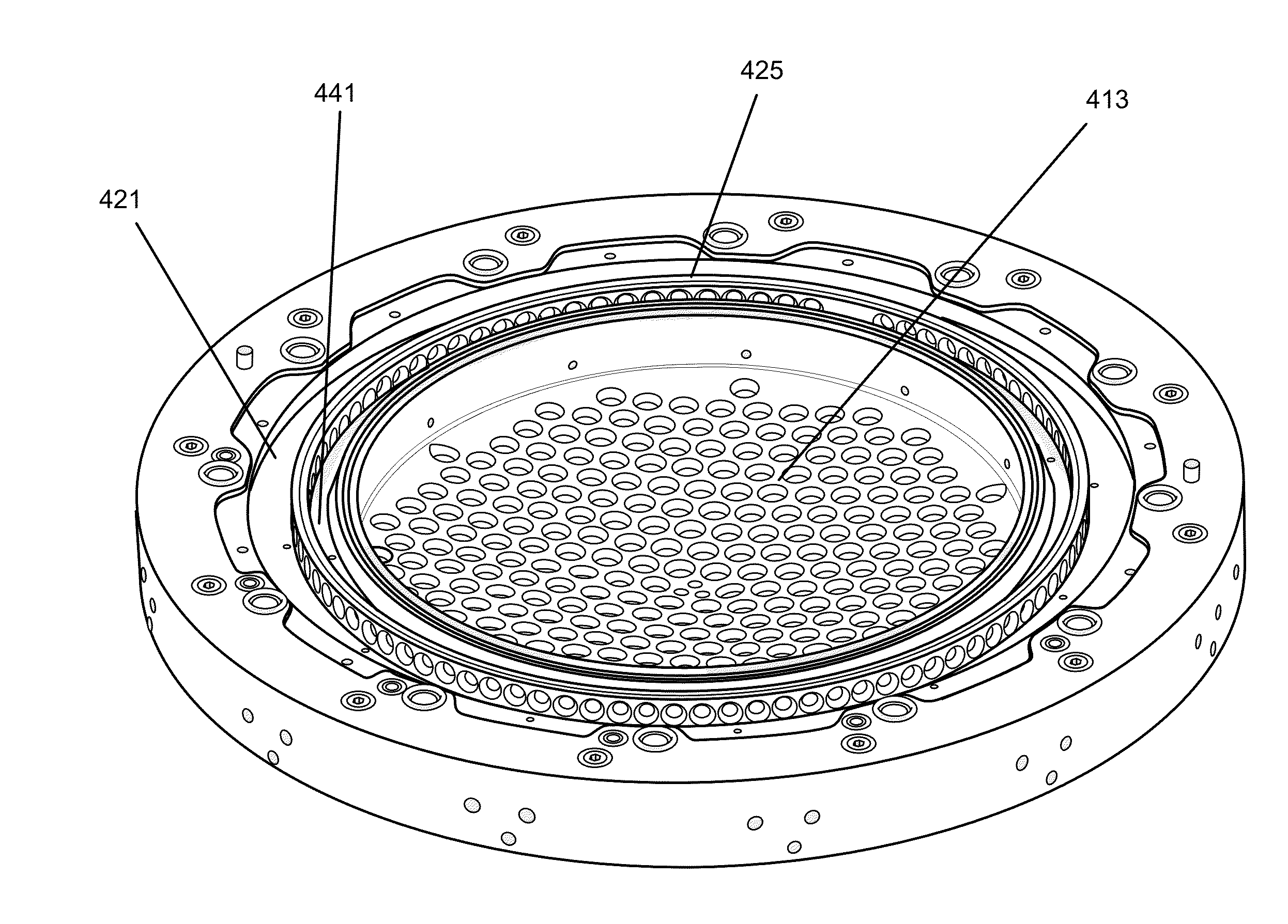
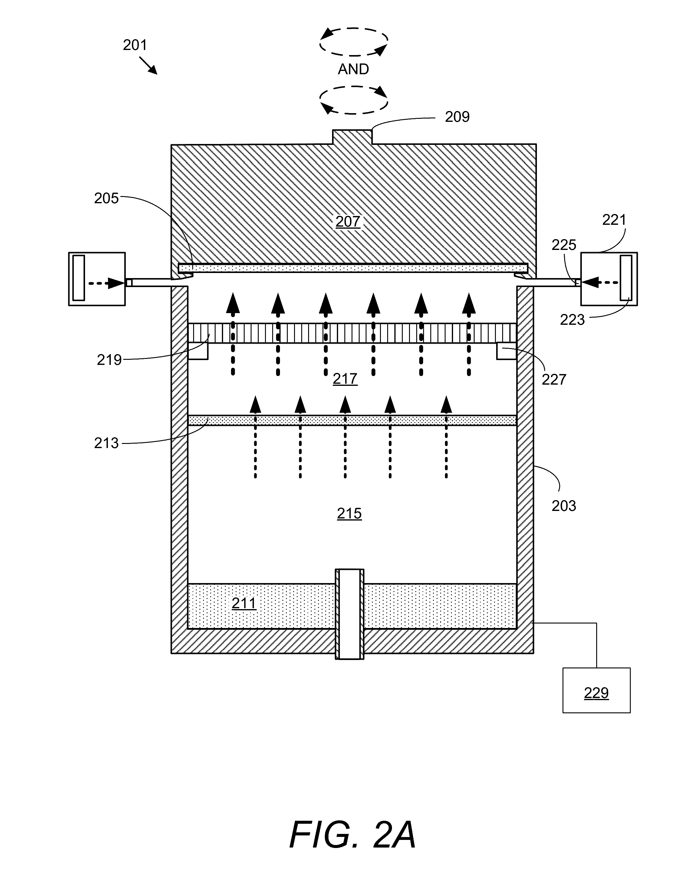
[0043]Methods and apparatus for electroplating a metal on a substrate while controlling uniformity of the electroplated layer, such as radial uniformity, azimuthal uniformity, or both, are provided. The methods are particularly useful for sequentially electroplating metal on dissimilar substrates, such as on semiconductor wafers having different patterns or distribution of recessed features on the surface. The methods control plating current (ionic current) at the substrate using a remotely positioned secondary electrode.

[0044]Embodiments are described generally where the substrate is a semiconductor wafer; however the invention is not so limited. Provided apparatus and methods are useful for electroplating metals in TSV and WLP applications, but can also be used in a variety of other electroplating processes, including deposition of copper in damascene features. Examples of metals that can be electroplated using provided methods include, without limitation, copper, silver, tin, ind...


PUM

PropertyMeasurementUnit
voltageaaaaaaaaaa
diameteraaaaaaaaaa
diameteraaaaaaaaaa

Abstract

An apparatus for electroplating metal on a substrate while controlling plating uniformity includes in one aspect: a plating chamber having anolyte and catholyte compartments separated by a membrane; a primary anode positioned in the anolyte compartment; an ionically resistive ionically permeable element positioned between the membrane and a substrate in the catholyte compartment; and a secondary electrode configured to donate and / or divert plating current to and / or from the substrate, wherein the secondary electrode is positioned such that the donated and / or diverted plating current does not cross the membrane separating the anolyte and catholyte compartments, but passes through the ionically resistive ionically permeable element. In some embodiments the secondary electrode is an azimuthally symmetrical anode (e.g., a ring positioned in a separate compartment around the periphery of the plating chamber) that can be dynamically controlled during electroplating.

Description

FIELD OF THE INVENTION[0001]The present disclosure relates generally to a method and apparatus for electroplating a metal layer on a semiconductor wafer. More particularly, the method and apparatus described herein are useful for controlling plating uniformity.BACKGROUND[0002]The transition from aluminum to copper in integrated circuit (IC) fabrication required a change in process “architecture” (to damascene and dual-damascene) as well as a whole new set of process technologies. One process step used in producing copper damascene circuits is the formation of a “seed-” or “strike-” layer, which is then used as a base layer onto which copper is electroplated (“electrofill”). The seed layer carries the electrical plating current from the edge region of the wafer (where electrical contact is made) to all trenches and via structures located across the wafer surface. The seed film is typically a thin conductive copper layer, though other conductive materials can be used depending on appl...

Claims


Application Information

Patent Timeline
Patent Type & Authority Applications(United States)
IPC IPC(8): C25D5/04C25D17/00
CPCC25D17/002C25D5/04C25D7/12C25D17/06C25D17/10C25F5/00C25D17/001C25D17/008C25D17/007C25D17/12C25D7/123
Inventor KAGAJWALA, BURHANUDDINBUCKALEW, BRYAN L.MAYER, STEVEN T.CHUA, LEE PENGBERKE, AARONFORTNER, JAMES ISAACRASH, ROBERT
Owner LAM RES CORP
Why Eureka
Try Eureka