Semiconductor device and method for manufacturing the same

a semiconductor and transistor technology, applied in the direction of semiconductor devices, electrical devices, transistors, etc., can solve the problems of affecting the reliability of transistors, the parasitic capacitance of transistors and in the vicinity of transistors is a major problem, and the various steps of manufacturing transistors are difficult to control, so as to achieve small parasitic capacitance, favorable electrical characteristics, and high frequency characteristics

Active Publication Date: 2016-08-11
SEMICON ENERGY LAB CO LTD
View PDF0 Cites 32 Cited by
  • Summary
  • Abstract
  • Description
  • Claims
  • Application Information

AI Technical Summary

Benefits of technology

[0031]A miniaturized transistor can be provided. A transistor with small parasitic capacitance can be provided. A transistor with high frequency characteristics can be provided. A transistor with favorable electrical characteristics can be provided. A transistor with stable electrical characteristics can be provided. A transistor with low off-state current can be pr...

Problems solved by technology

In miniaturization of a semiconductor element, the parasitic capacitance in a transistor and in the vicinity of the transistor is a major problem.
It becomes more difficult to control various steps of manufact...

Method used


Image

  • Semiconductor device and method for manufacturing the same
  • Semiconductor device and method for manufacturing the same
  • Semiconductor device and method for manufacturing the same

Examples


embodiment 1

[0092]In this embodiment, examples of a transistor which is a semiconductor device of an embodiment of the present invention and an example of a method for manufacturing the transistor will be described.

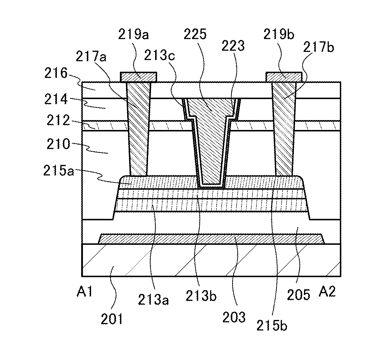
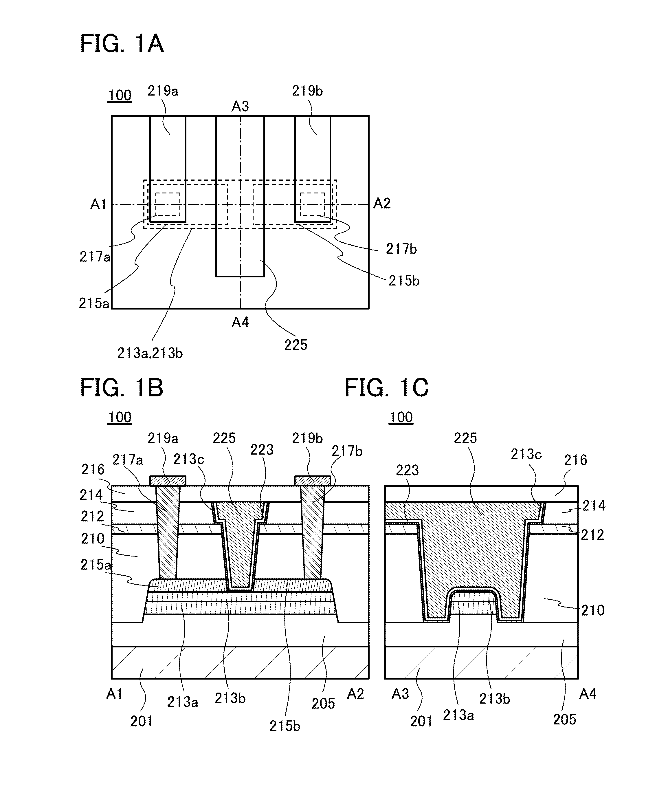
[0093]FIGS. 1A to 1C illustrate a transistor 100 of an embodiment of the present invention. FIG. 1A is a top view of the transistor 100, FIG. 1B is a cross-sectional view taken along dashed-dotted line A1-A2 in FIG. 1A, and FIG. 1C is a cross-sectional view taken along dashed-dotted line A3-A4 in FIG. 1A. The transistor 100 includes a substrate 201; an insulator 205; a semiconductor 213a; a semiconductor 213b; a semiconductor 213c; a conductor 215a; a conductor 215b; an insulator 223; a conductor 225; an insulator 210; an insulator 212; an insulator 214; an insulator 216; a conductor 217a; a conductor 217b; a conductor 219a; and a conductor 219b.

[0094]The conductor 225 functions as a gate electrode of the transistor 100. The conductors 215a and 215b function as a source electrode an...

embodiment 2

[0220]In this embodiment, a method for manufacturing a transistor, which is partly different from that of the transistor in Embodiment 1, is described. The transistor in this embodiment differs from the transistor in Embodiment 1 in that a conductor functioning as a source electrode and a drain electrode also functions as a wiring.

[0221]FIG. 15A, FIG. 16A, FIG. 17A, FIG. 18A, and FIG. 19A are top views illustrating a method for manufacturing a transistor. FIG. 15B, FIG. 16B, FIG. 17B, FIG. 18B, and FIG. 19B are each a cross-sectional view taken along dashed-dotted line A1-A2 shown in the corresponding top view. FIG. 15C, FIG. 16C, FIG. 17C, FIG. 18C, and FIG. 19C are each a cross-sectional view taken along dashed-dotted line A3-A4 shown in the corresponding top view. Note that for portions shown by the same reference numerals in the other embodiment, refer to the description in the other embodiment.

[0222]First, the substrate 201 is prepared.

[0223]Next, the insulator 205 is formed.

[0...

embodiment 3

[0243]In this embodiment, a method for manufacturing a transistor, which is partly different from any of the methods for manufacturing the transistors in Embodiments 1 and 2, is described.

[0244]FIG. 20A, FIG. 21A, FIG. 22A, FIG. 23A, and FIG. 24A are top views illustrating a method for manufacturing a transistor. FIG. 20B, FIG. 21B, FIG. 22B, FIG. 23B, and FIG. 24B are each a cross-sectional view taken along dashed-dotted line A1-A2 shown in the corresponding top view. FIG. 20C, FIG. 21C, FIG. 22C, FIG. 23C, and FIG. 24C are each a cross-sectional view taken along dashed-dotted line A3-A4 shown in the corresponding top view. Note that for portions shown by the same reference numerals in the other embodiment, refer to the description in the other embodiment.

[0245]First, the steps up to the step which is illustrated in FIGS. 3A to 3C and described in Embodiment 1 are performed.

[0246]Next, the insulator 211 is formed over the insulator 209 (see FIGS. 20A to 20C).

[0247]Next, a resist or...


PUM


Abstract

A semiconductor device is formed in such a manner that a first insulator, a first oxide semiconductor, and a first conductor are formed; the first conductor is processed to form a second conductor; the first oxide semiconductor is processed to form a second oxide semiconductor; a second insulator is formed over the second conductor; a third insulator is formed over the second insulator; a fourth insulator is formed over the third insulator; the fourth insulator, the third insulator, the second insulator, and the second conductor are selectively processed to partly expose the second oxide semiconductor; a fifth insulator is formed over the second oxide semiconductor and the fourth insulator; and a third conductor is formed over the fifth insulator and then chemical mechanical polishing treatment is performed to expose a top surface of the fourth insulator.

Description

BACKGROUND OF THE INVENTION[0001]1. Field of the Invention[0002]The present invention relates to, for example, a transistor and a semiconductor device. The present invention relates to, for example, a method for manufacturing a transistor and a semiconductor device. The present invention relates to, for example, a display device, a light-emitting device, a lighting device, a power storage device, a memory device, an imaging device, a processor, and an electronic device. The present invention relates to a method for manufacturing a display device, a liquid crystal display device, a light-emitting device, a memory device, an imaging device, and an electronic device. The present invention relates to a driving method of a display device, a liquid crystal display device, a light-emitting device, a memory device, an imaging device, or an electronic device.[0003]Note that one embodiment of the present invention is not limited to the above technical field. The technical field of one embodim...

Claims


Application Information

Patent Timeline
IPC IPC(8): H01L29/786H01L21/465H01L21/4763H01L29/66
CPCH01L29/7869H01L21/4763H01L21/465H01L29/66969H01L21/76805H01L2221/1031H01L27/1225H01L27/1207H01L29/42384H01L29/78696
Inventor OKAZAKI, YUTAKA
Owner SEMICON ENERGY LAB CO LTD
Why Eureka
Try Eureka