COMPOSITION FOR FORMING CONDUCTIVE PATTERN AND RESIN STRUCTURE HAVING CONDUCTIVE PATTERN THEREON (As Amended)

Active Publication Date: 2016-08-11
LG CHEM LTD
View PDF1 Cites 2 Cited by
  • Summary
  • Abstract
  • Description
  • Claims
  • Application Information

AI Technical Summary

Benefits of technology

[0025]According to the present invention, a composition for forming a conductive pattern which is capable of forming a fine conductive pattern on a polymeric resin substrate such as a variety of polymeric resin products or resin layers by a very simplified process of electromagnetic irradiation such as laser irradiation, a method for forming the conductive pattern using the same, and a resin structure having the conductive pattern obtained therefrom may be provided.
[0026]In particular, as the composition for forming the conductive pattern according to the present invention and the like use a non-conductive metal compound having a specific three-dimensional structure, and the like, an excellent fine conductive pattern having excellent adhesion strength may be mor

Problems solved by technology

However, a more effective method for these technologies has not been suggested yet.
However, when the conductive pattern is formed according to this technology, there are limitations that a process or equipment to be needed becomes too complicated, or it is difficult to form an excellent fine conductive pattern.
However, when the conductive pattern is formed by the above technology, the conductive pattern has poor adhesion strength to the poly

Method used


Image

  • COMPOSITION FOR FORMING CONDUCTIVE PATTERN AND RESIN STRUCTURE HAVING CONDUCTIVE PATTERN THEREON (As Amended)
  • COMPOSITION FOR FORMING CONDUCTIVE PATTERN AND RESIN STRUCTURE HAVING CONDUCTIVE PATTERN THEREON (As Amended)
  • COMPOSITION FOR FORMING CONDUCTIVE PATTERN AND RESIN STRUCTURE HAVING CONDUCTIVE PATTERN THEREON (As Amended)

Examples


preparation example 1

Synthesis of Non-Conductive Metal Compound CuCrO2

[0087]Raw materials, CuO and Cr2O3 were uniformly mixed with each other at a molar ratio of 2:1 by ball milling for 6 hours. Thereafter, the mixture was calcined under conditions of atmospheric pressure and 1050° C. for 2 hours to synthesize powders having Chemical Formula of CuCrO2. After the synthesis, CuCrO2 powders having controlled particle size to be used in the following Examples were prepared by controlling milling time for comminution process. An electron micrograph and an X-ray diffraction pattern of the CuCrO2 powder are shown in FIGS. 4 and 5, respectively.

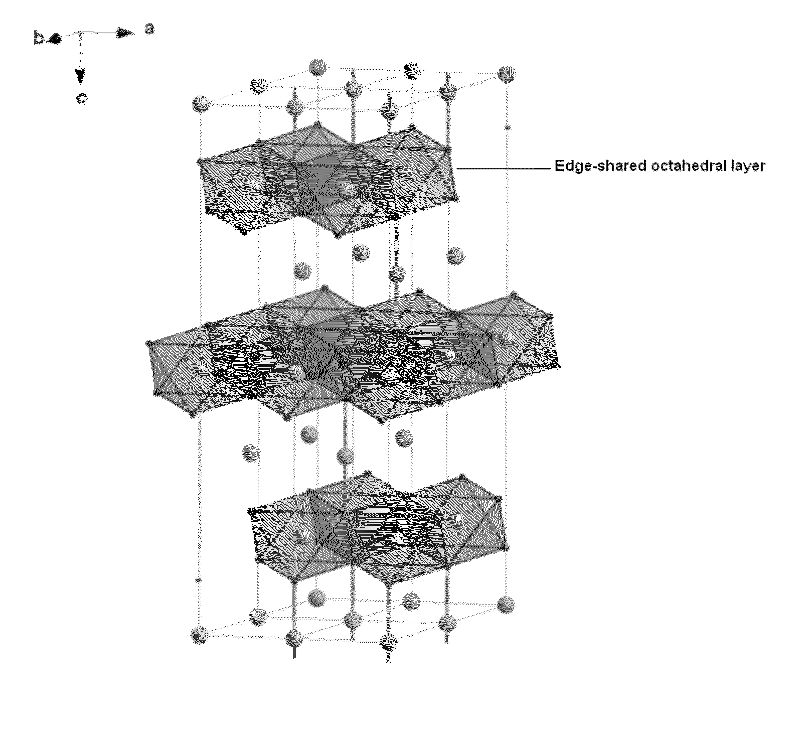
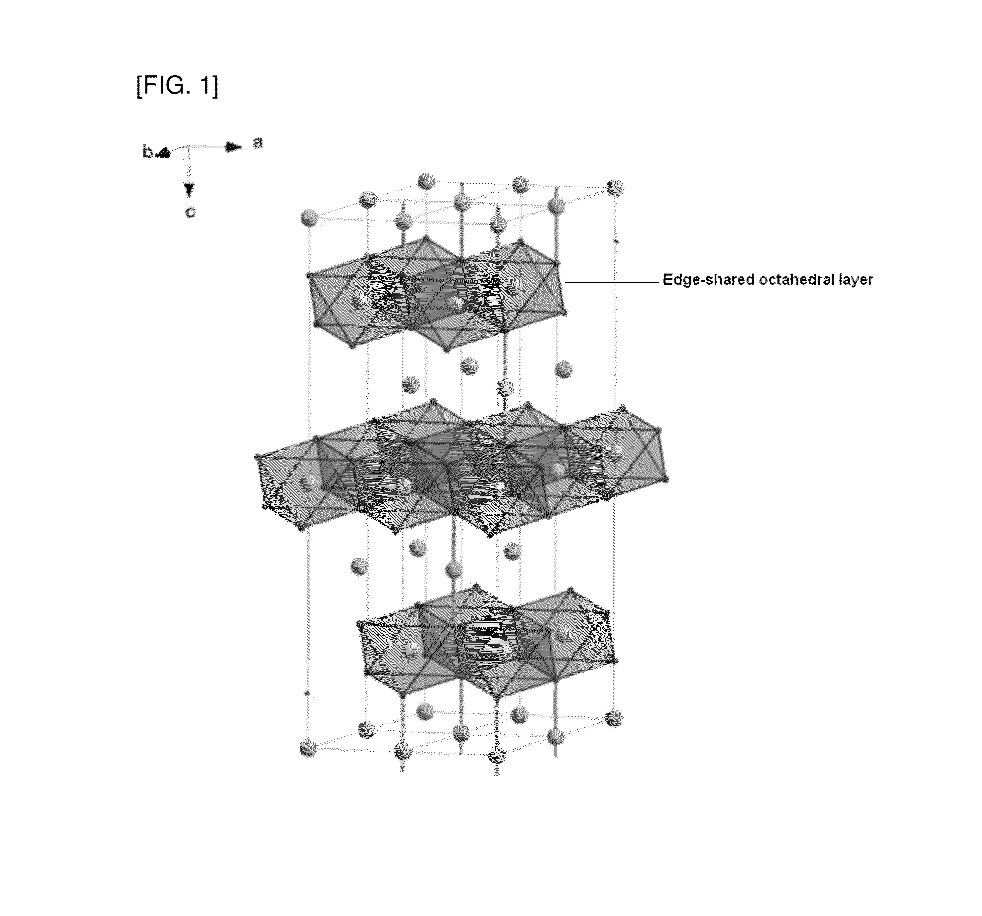
[0088]The electron microscope and X-ray diffraction analysis showed that the non-conductive metal compound has a flat-type crystal structure, and the layered three-dimensional structure (a R3m or P63 / mmc space group in crystal structure) as illustrated in FIG. 1.

examples 1 to 3

Formation of Conductive Pattern by Direct Laser Irradiation

[0089]A composition for forming a conductive pattern by electromagnetic wave irradiation was prepared by using a polycarbonate resin as a base resin, non-conductive metal compound particles (CuCrO2; average particle size: 0.5 μm) obtained by Preparation Example 1 as an LDS additive, together with additives for the process and stabilization.

[0090]As the additives, trialkyl phosphate as a commercialized flame retardant, a heat stabilizer (IR1076, PEP36), a UV stabilizer (UV329), a lubricant (EP184), and an impact modifier (S2001) were used.

[0091]As shown in Table 1 below, 79 to 84 wt % of the polycarbonate resin, and 3 to 5 wt % of the LDS additive of the Preparation Example 1 (CuCrO2; average particle size: 0.5 μm) were used, and 6 to 11 wt % of the flame retardant, 4 wt % of the impact modifier, and 1 wt % of other additives including the lubricant were added to be mixed to obtain the composition, which was extruded by an ex...

experimental example 1

Evaluation on Reflectivity of Resin Structure to Laser and Evaluation on Adhesion Strength of Conductive Pattern

[0102]First, in Examples 1 to 3 and Comparative Examples 1 and 2, reflectivity to the laser with a wavelength of 1064 nm in the resin substrate immediately before laser irradiation was measured using a UV-vis-NIR spectrometer. The measurement results are summarized in following Table 2.

[0103]Referring to Table 2 below, it was found that the substrates of Examples 1 to 3 showed relatively low reflectivity to the laser, indicating high absorption and sensitivity to the laser, whereas the substrate of Comparative Examples 1 and 2 showed high reflectivity, that is, low absorption and sensitivity to the laser. It was confirmed therefrom that formation of the metal nucleus and better conductive pattern is possible by using the compositions of Examples, as compared to the composition of Comparative Examples 1 and 2.

[0104]Then, after the conductive pattern was formed in Examples 1...


PUM

PropertyMeasurementUnit
Fractionaaaaaaaaaa
Fractionaaaaaaaaaa
Poweraaaaaaaaaa

Abstract

The present invention relates to a composition for forming a conductive pattern which is capable of forming a fine conductive pattern on a variety of polymeric resin products or resin layers by a simplified process, while imparting excellent flame retardancy to the resin products or resin layers, and a resin structure having the conductive pattern obtained using the composition. The composition for forming a conductive pattern includes: a polymer resin; a non-conductive metal compound including a first metal element and a second metal element, having a R3m or P63/mmc space group in crystal structure; and a flame retardant, wherein a metal nucleus including the first metal element, the second metal element or an ion thereof is formed from the non-conductive metal compound by the electromagnetic irradiation.

Description

TECHNICAL FIELD[0001]The present invention relates to a composition for forming a conductive pattern which is capable of forming an excellent fine conductive pattern on a variety of polymeric resin products or resin layers by a simplified process, while imparting excellent flame retardancy to the resin products or resin layers, and a resin structure having the conductive pattern obtained therefrom.BACKGROUND[0002]With the recent development of microelectronic technology, a need for structures having a fine conductive pattern formed on the surface of a polymeric resin substrate (or product) such as a variety of resin products or resin layers has grown. The conductive patterns on the surface of the polymeric resin substrate and the structure may be applied to form various objects such as antennas integrated into a mobile phone case, a variety of sensors, MEMS structures, RFID tags, and the like.[0003]As such, with increasing interest in the technology of forming the conductive pattern...

Claims


Application Information

Patent Timeline
IPC IPC(8): H05K1/03H05K3/00H01B1/22H05K3/10
CPCH05K2201/012H05K3/10H05K3/0055H05K1/0373H05K1/0326H01B1/22H05K2201/0145H05K2201/0129C09D5/24C09D201/00H05K2201/0158C08K3/24C08K5/521C08L69/00H01B5/14H01B13/00H05K1/0201C08K3/22
Inventor JUN, SHIN HEEPARK, CHEE-SUNGKIM, JAE HYUNJUNG, SANG YUNPARK, CHEOL-HEEJEONG, HAN NAH
Owner LG CHEM LTD
Why Eureka
Try Eureka