

Semiconductor device and display device including the semiconductor device
- Summary
- Abstract
- Description
- Claims
- Application Information
AI Technical Summary
Benefits of technology
Problems solved by technology
Method used
Image

Examples
embodiment 1
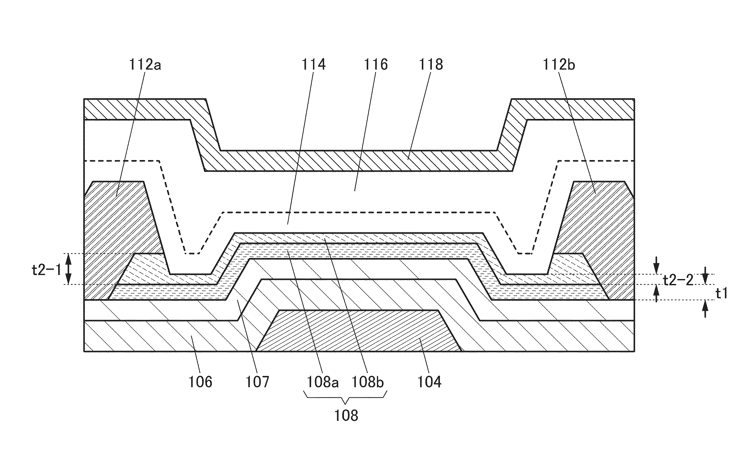
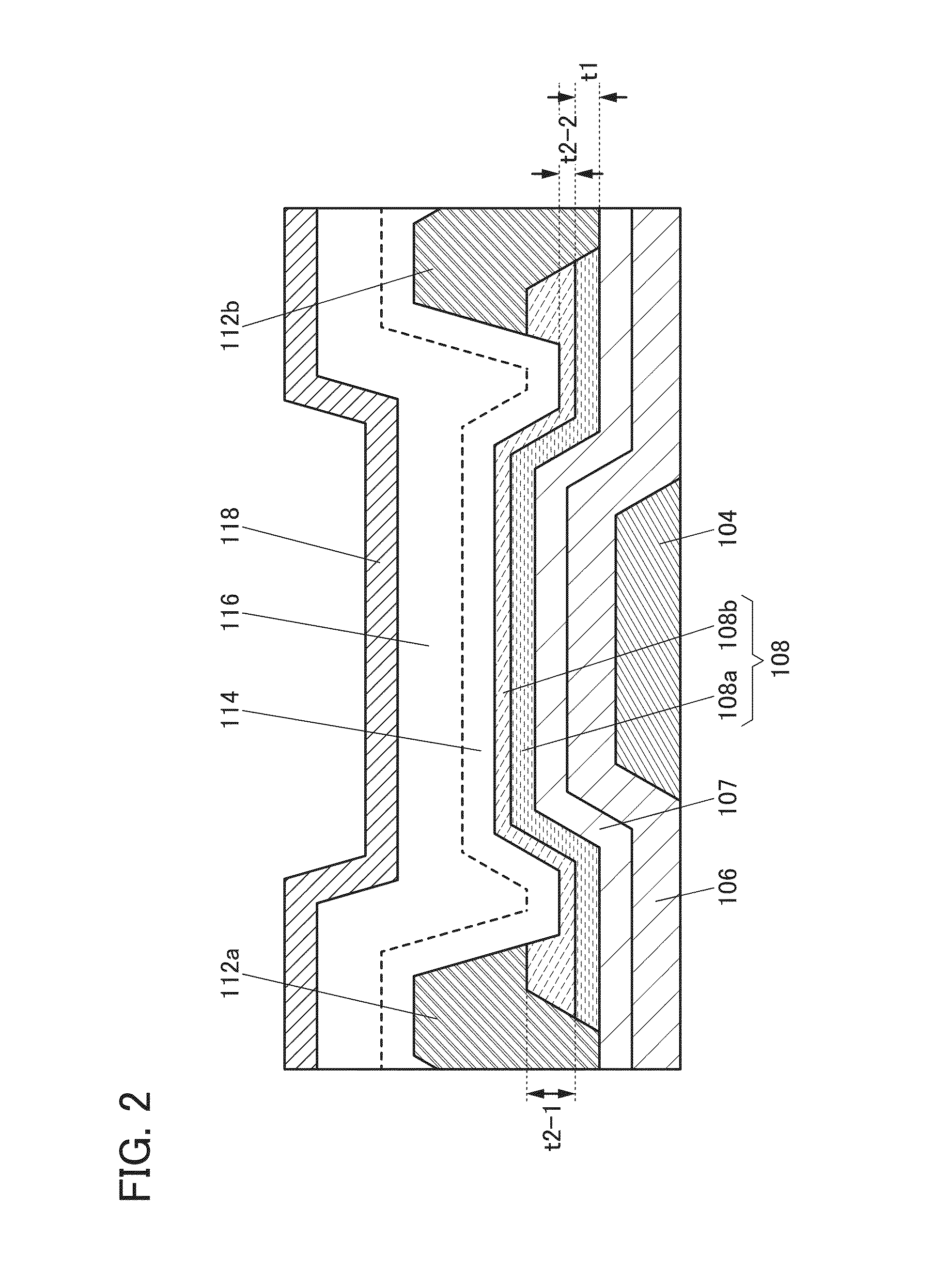
[0095]In this embodiment, a semiconductor device that is one embodiment of the present invention and a method of manufacturing the semiconductor device are described with reference to FIGS. 1A to 1C, FIG. 2, FIGS. 3A to 3C, FIGS. 4A to 4D, FIGS. 5A to 5D, FIGS. 6A to 6C, FIGS. 7A to 7H, FIGS. 10A to 10C, FIGS. 11A-1, 11A-2, 11B-1, and 11B-2, FIGS. 12A-1, 12A-2, 12B-1, and 12B-2, FIGS. 13A-1, 13A-2, 13B-1, and 13B-2, FIGS. 14A-1, 14A-2, 14B-1, and 14B-2, FIGS. 15A-1, 15A-2, 15B-1, and 15B-2, FIGS. 16A-1, 16A-2, 16B-1, and 16B-2, FIGS. 17A-1, 17A-2, 17B-1, and 17B-2, and FIGS. 18A-1, 18A-2, 18B-1, and 18B-2.
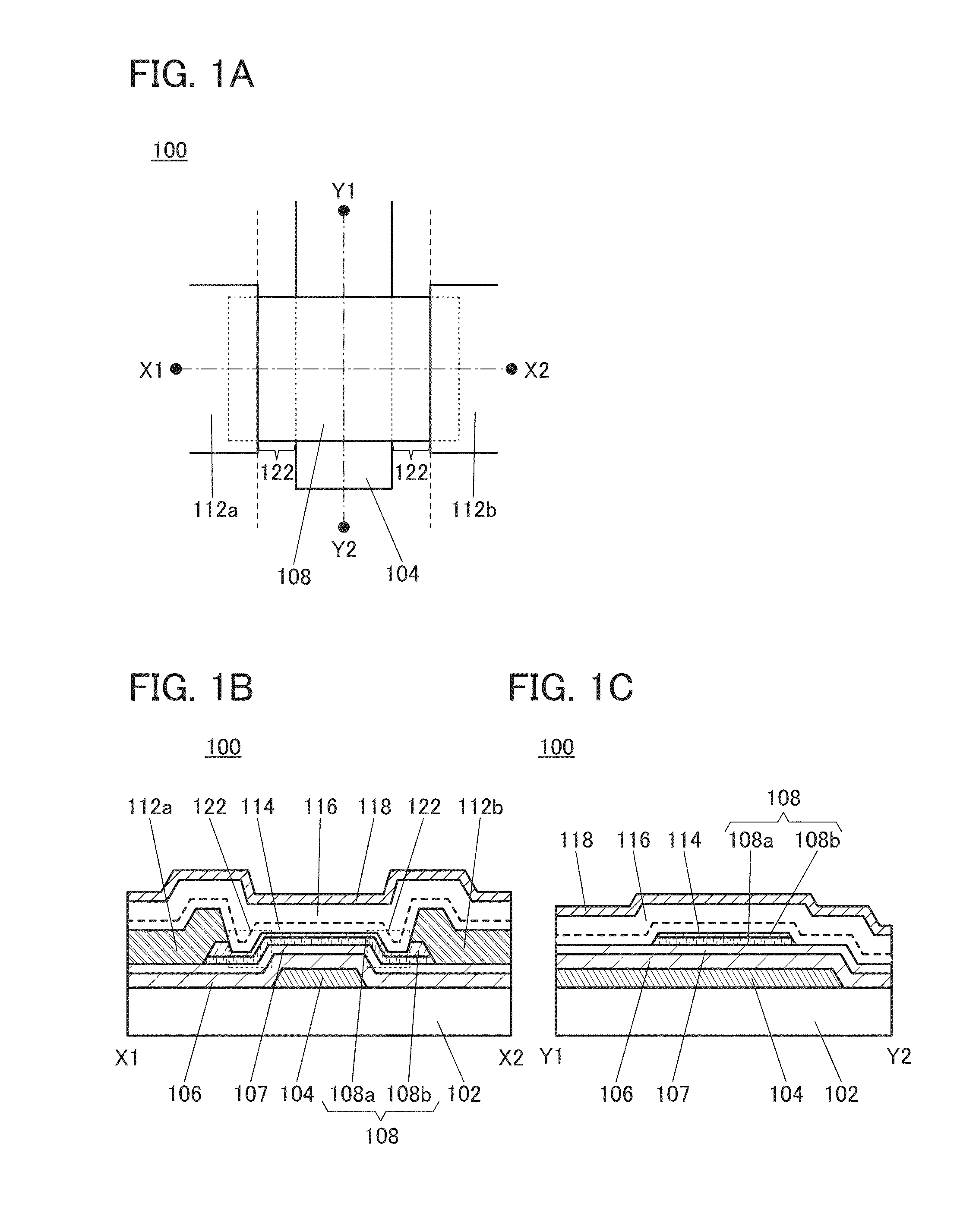
[0096]FIG. 1A is a top view of a transistor 100 that is a semiconductor device of one embodiment of the present invention. FIG. 1B is a cross-sectional view taken along a dashed-dotted line X1-X2 in FIG. 1A. FIG. 1C is a cross-sectional view taken along a dashed-dotted line Y1-Y2 in FIG. 1A. Note that in FIG. 1A, some components of the transistor 100 (e.g., an insulating film servi...
embodiment 2
[0305]In this embodiment, the structure of an oxide semiconductor included in a semiconductor device of one embodiment of the present invention will be described in detail.
[0306]An oxide semiconductor is classified into a single crystal oxide semiconductor and a non-single-crystal oxide semiconductor. Examples of a non-single-crystal oxide semiconductor include a c-axis aligned crystalline oxide semiconductor (CAAC-OS), a polycrystalline oxide semiconductor, a nanocrystalline oxide semiconductor (nc-OS), an amorphous-like oxide semiconductor (a-like OS), and an amorphous oxide semiconductor.
[0307]From another perspective, an oxide semiconductor is classified into an amorphous oxide semiconductor and a crystalline oxide semiconductor. Examples of a crystalline oxide semiconductor include a single crystal oxide semiconductor, a CAAC-OS, a polycrystalline oxide semiconductor, and an nc-OS.
[0308]It is known that an amorphous structure is generally defined as being metastable and unfixed...
embodiment 3
[0375]In this embodiment, an example of a display device that includes any of the transistors described in the above embodiment will be described below with reference to FIG. 27, FIG. 28, and FIG. 29.
[0376]FIG. 27 is a top view of an example of a display device. A display device 700 illustrated in FIG. 27 includes a pixel portion 702 provided over a first substrate 701; a source driver circuit portion 704 and a gate driver circuit portion 706 provided over the first substrate 701; a sealant 712 provided to surround the pixel portion 702, the source driver circuit portion 704, and the gate driver circuit portion 706; and a second substrate 705 provided to face the first substrate 701. The first substrate 701 and the second substrate 705 are sealed with the sealant 712. That is, the pixel portion 702, the source driver circuit portion 704, and the gate driver circuit portion 706 are sealed with the first substrate 701, the sealant 712, and the second substrate 705. Although not illust...
PUM
 Abstract
Description
Claims
Application Information