

Method of forming copper interconnects
a technology of copper interconnects and copper interconnects, which is applied in the direction of semiconductor/solid-state device manufacturing, basic electric elements, electric devices, etc., can solve the problems of reducing the performance of copper interconnect devices of sub-40 nm technology nodes, reducing the reliability requirements of devices, and risking process stability, so as to reduce the effective thickness of copper interconnects, reduce the effect of erosion and polishing residues, and reduce the defect of effective thickness
- Summary
- Abstract
- Description
- Claims
- Application Information
AI Technical Summary
Benefits of technology
Problems solved by technology
Method used
Image

Examples
first embodiment
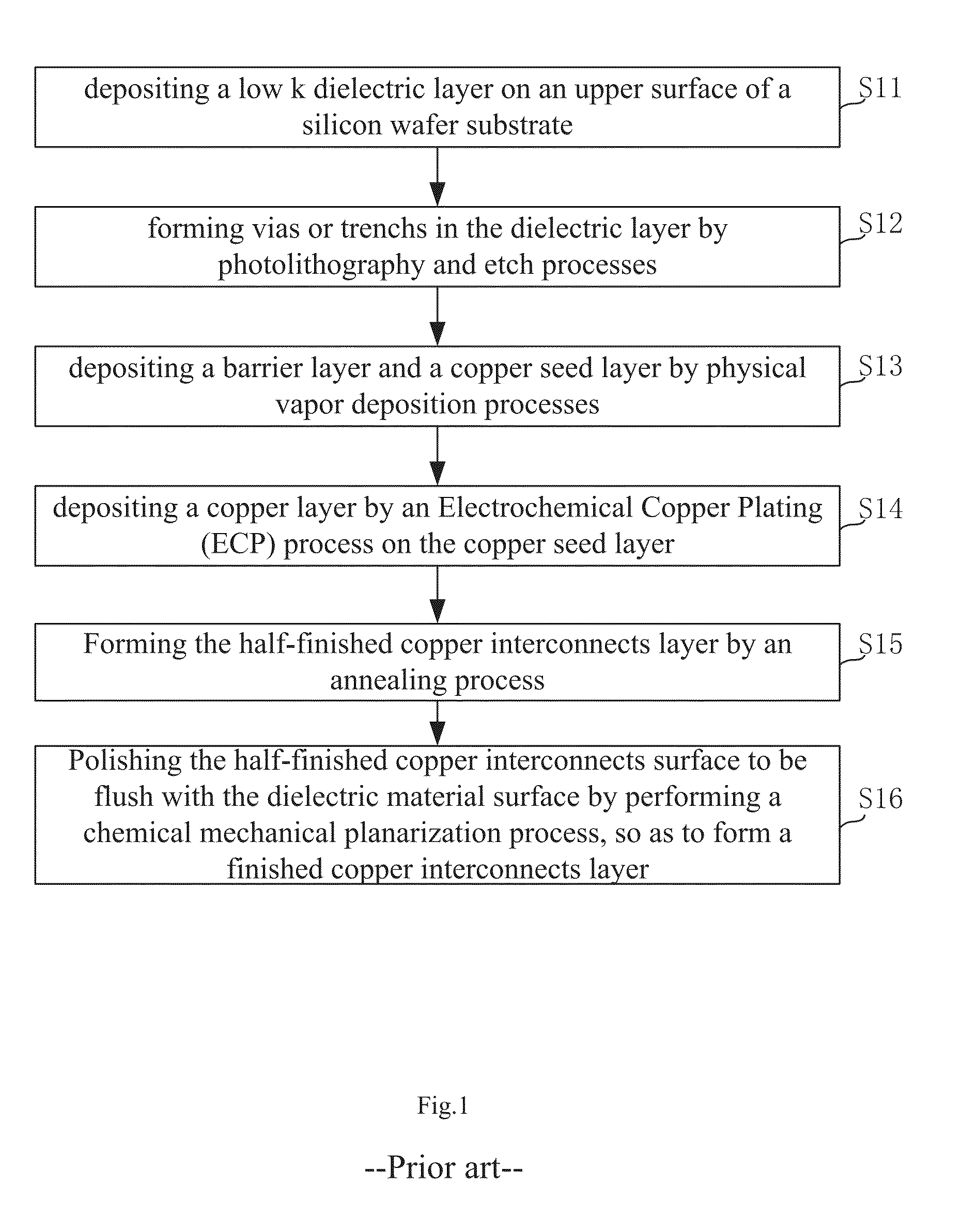
[0057]FIG. 8 is a flow chart illustrating a method of forming copper interconnects according to the present invention; as shown in FIG. 8, the method of forming copper interconnects includes the following steps:
[0058]Step S81: depositing a dielectric layer on a silicon wafer substrate.
[0059]In the step S81 of the embodiment, a dielectric layer is formed by depositing a low k dielectric material; the low k dielectric material is Black Diamond series or SiLK series and the relative dielectric constant k value thereof is between 2.2 and 3.0. When Black Diamond series II is used as the dielectric material, the k value is between 2.5 and 2.6.
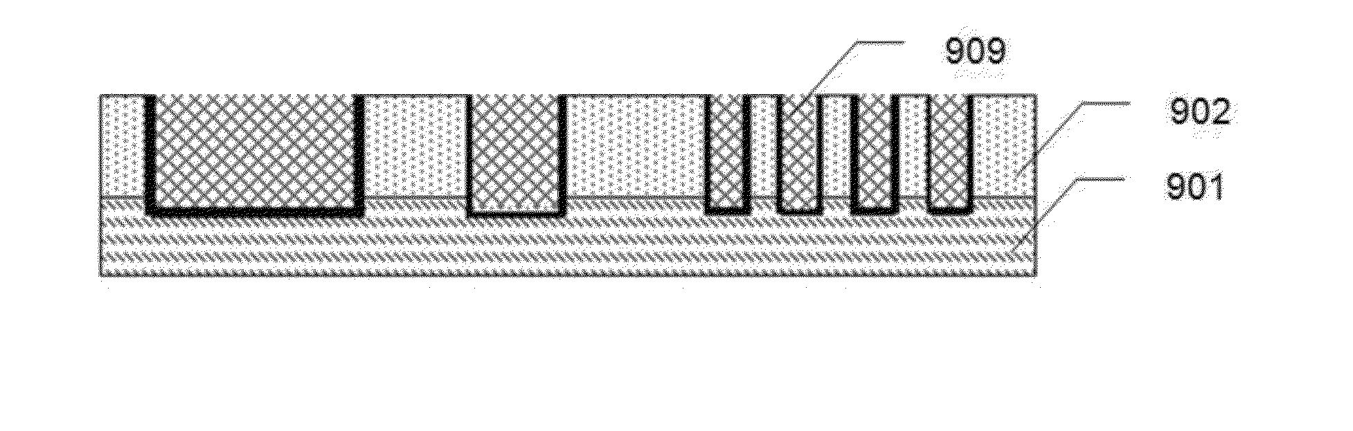
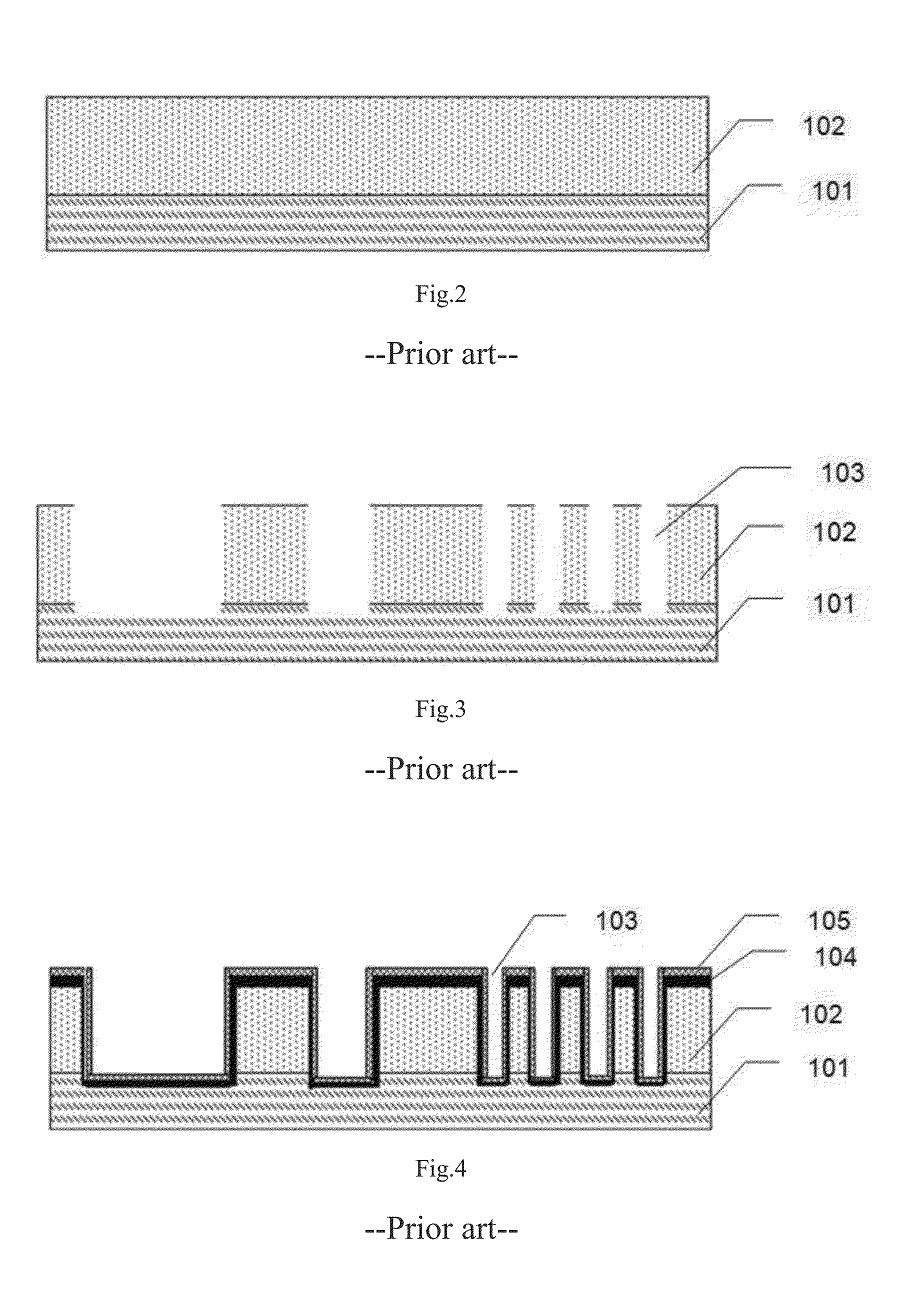
[0060]FIG. 9 is a sectional view of structure of the semi-manufactured product after step S81; as shown in FIG. 9, a dielectric layer 902 is deposited on a silicon wafer substrate 901.
[0061]Step S82: forming vias and / or trenches in the dielectric layer.
[0062]FIG. 10 is a sectional view of structure of the semi-manufactured product after step S82; as ...
second embodiment
[0090]FIG. 17 is a flow chart illustrating the method of forming copper interconnects according to the present invention; as shown in FIG. 17, the method of forming copper interconnects includes the following steps:
[0091]Step S91: depositing a dielectric layer on a silicon wafer substrate;
[0092]Step S92: forming vias and / or trenches in the dielectric layer;
[0093]Step S93: depositing a barrier layer and a copper seed layer sequentially from bottom to top on the upper surface of the dielectric layer;
[0094]Step S94: depositing a copper layer on the copper seed layer to form copper interconnects (unannealed);
[0095]Step S95: performing an annealing process;
[0096]Step S96: performing a multi-step polishing process to remove the bulk coppers and stopping at the barrier layer;
[0097]The details of steps S91 to S96 can be seen in the steps S81 to S86 of the first embodiment, no further detailed explanation is deemed necessary herein.
[0098]Step S97: forming a copper repair layer by depositing ...
PUM
 Abstract
Description
Claims
Application Information