

Hybrid high electron mobility transistor and active matrix structure
- Summary
- Abstract
- Description
- Claims
- Application Information
AI Technical Summary
Benefits of technology
Problems solved by technology
Method used
Image

Examples
Embodiment Construction
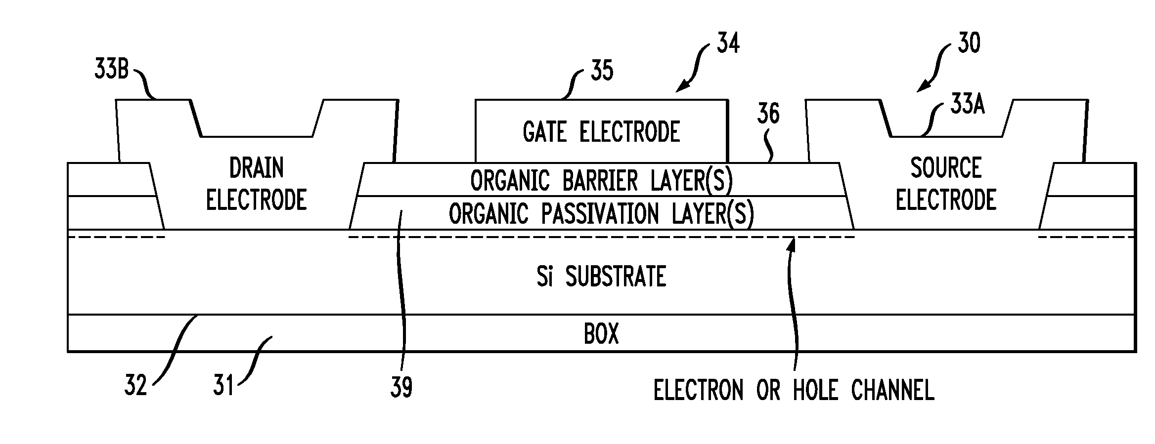
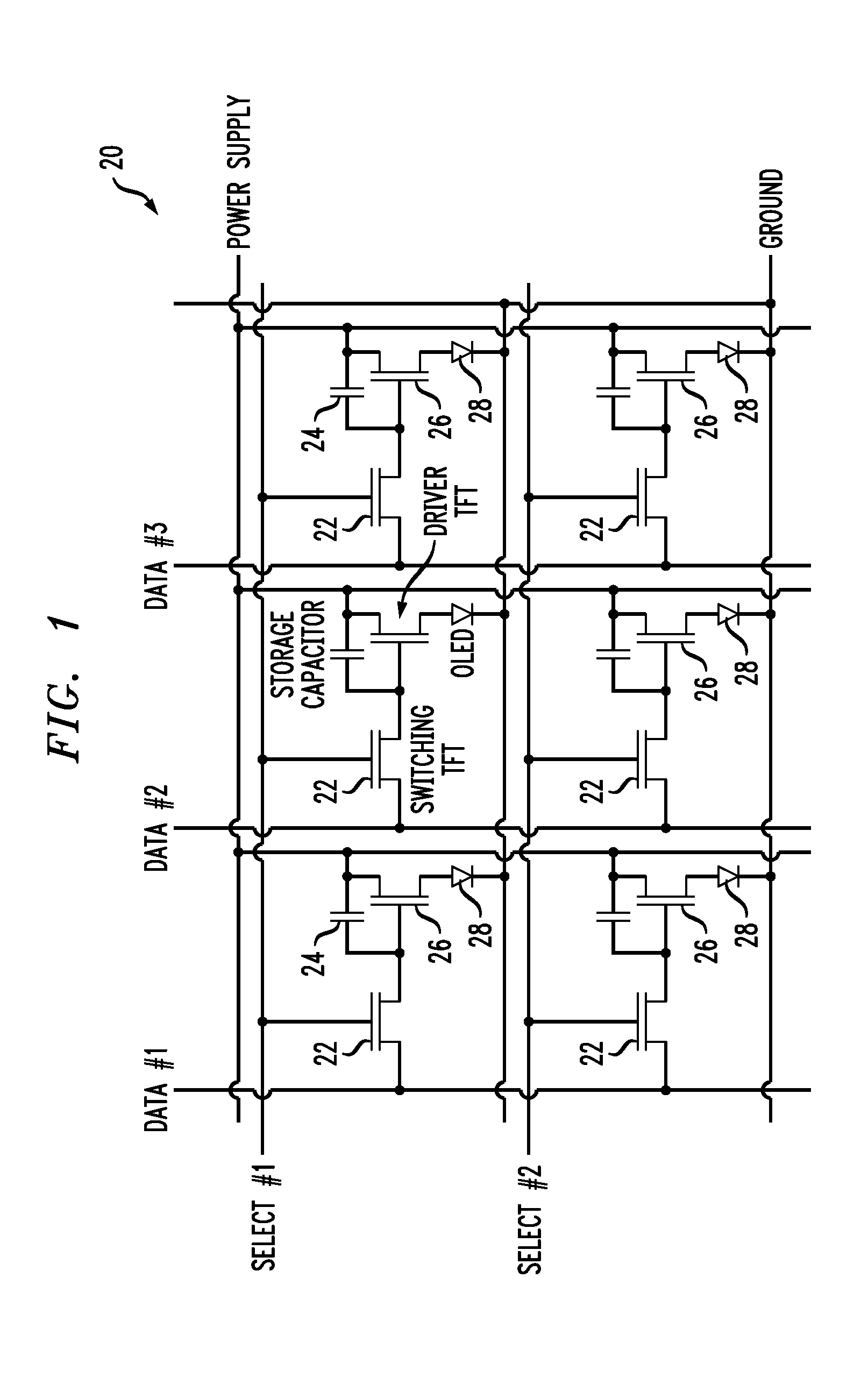
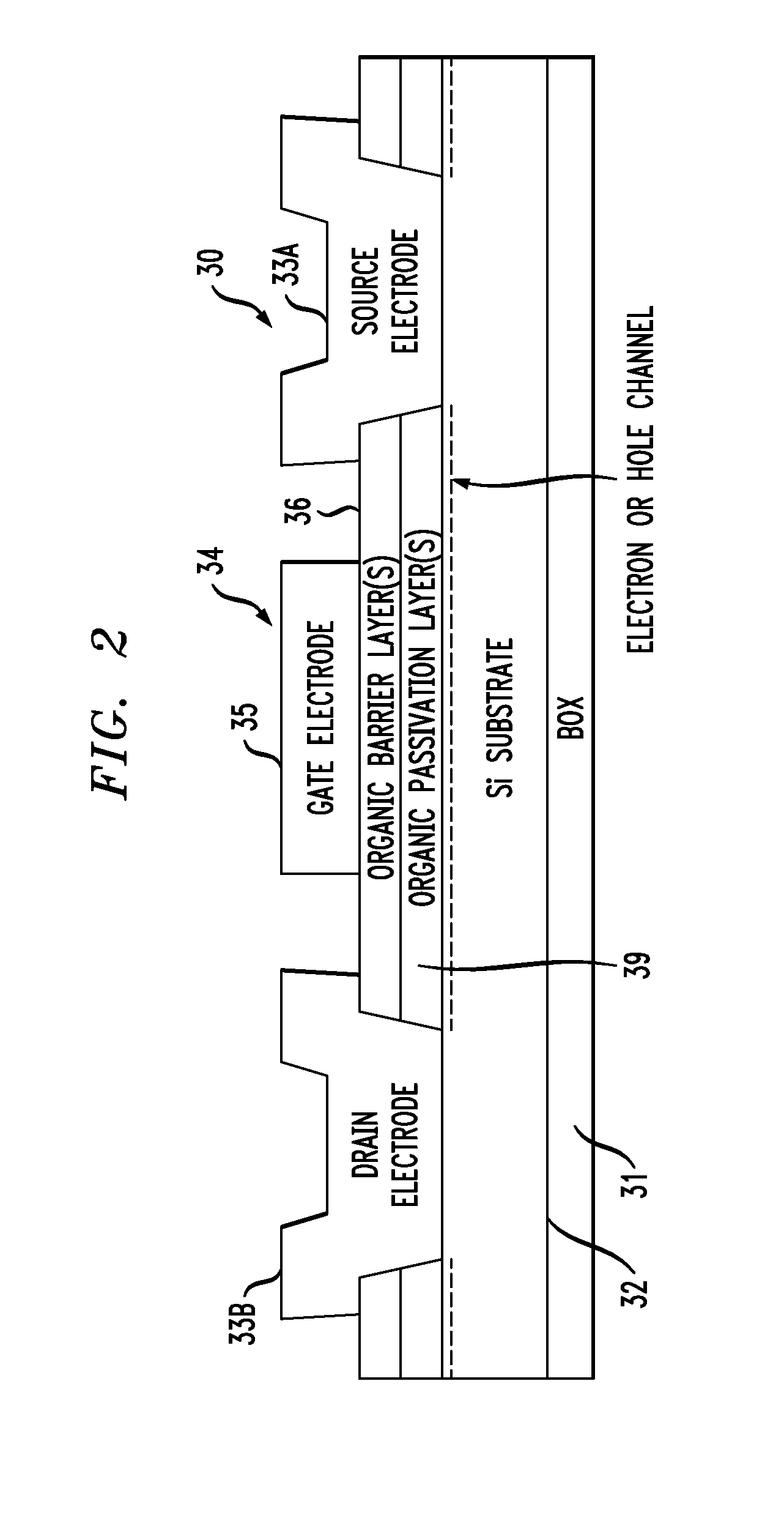
[0036]Thin-film hybrid high electron mobility transistors (HEMTs) are disclosed that include crystalline, inorganic semiconductor channels and organic gate barrier layers. Such transistors are used in some embodiments for forming high resolution active matrix displays. A backplane refers to an array of transistors (active devices) used for addressing and programming passive devices such as light emitting diodes, liquid crystal displays, photosensitive materials (e.g. for x-ray imaging), or sensors (e.g. piezoelectric materials for sensing pressure). The backplane also contains address lines, program lines, power supply lines, and typically storage capacitors which are fabricated using the same process technology as that of the transistors. Arrays of passive devices addressed / programmed by the backplane are typically referred to as the frontplane. An active matrix refers to the combination of a backplane and a frontplane. Schematic pixel circuits of active-matrix arrays comprised of ...
PUM
 Abstract
Description
Claims
Application Information