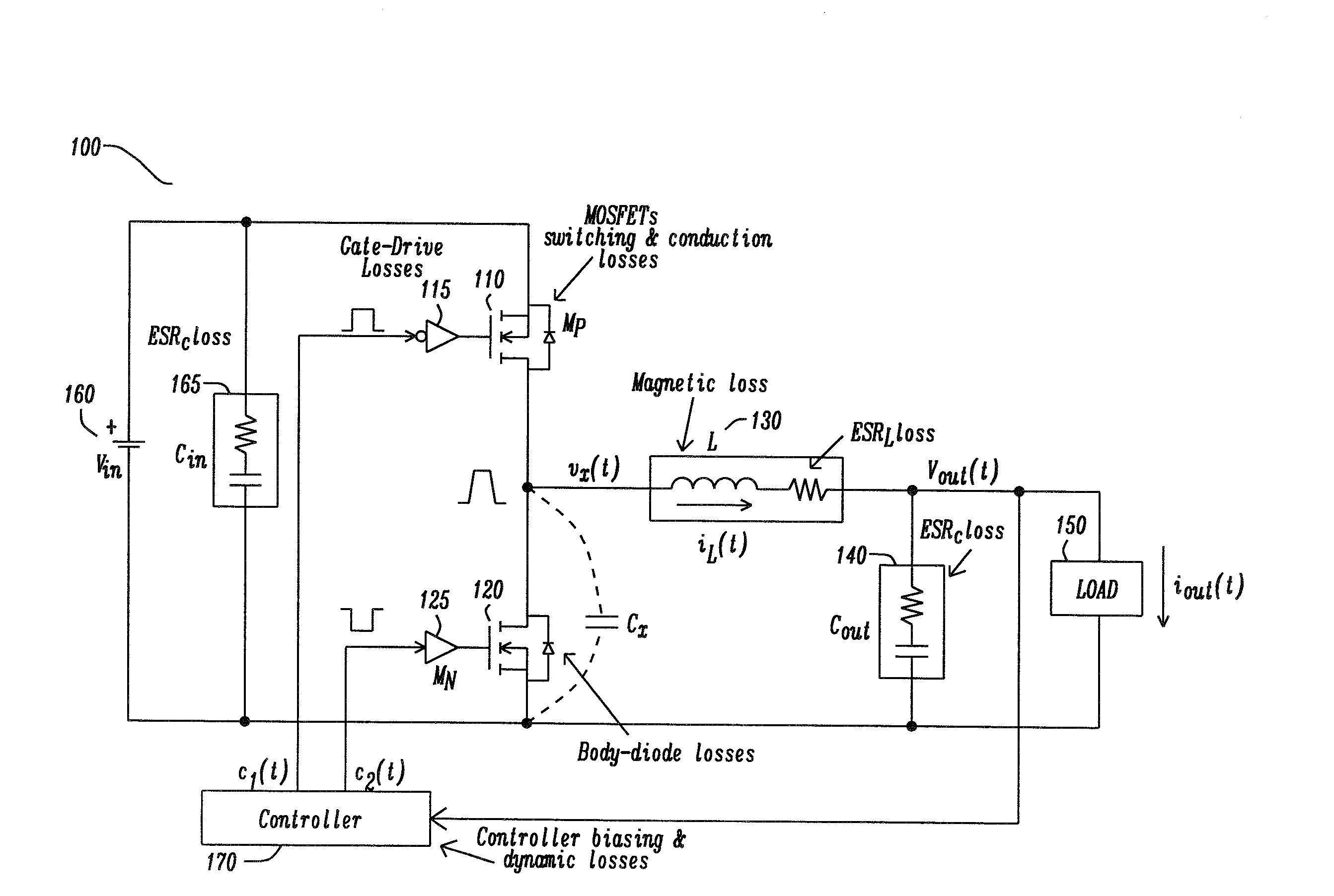
High Efficiency DC-to-DC Converter with Adaptive Output Stage
a converter and output stage technology, applied in the direction of power conversion systems, electric variable regulation, instruments, etc., can solve the problems of low output voltage regulation, low efficiency, and significant losses of mosfet switching and gate-drives, and achieve the effect of minimal power loss
- Summary
- Abstract
- Description
- Claims
- Application Information
AI Technical Summary
Benefits of technology
Problems solved by technology
Method used
Image

Examples
first embodiment
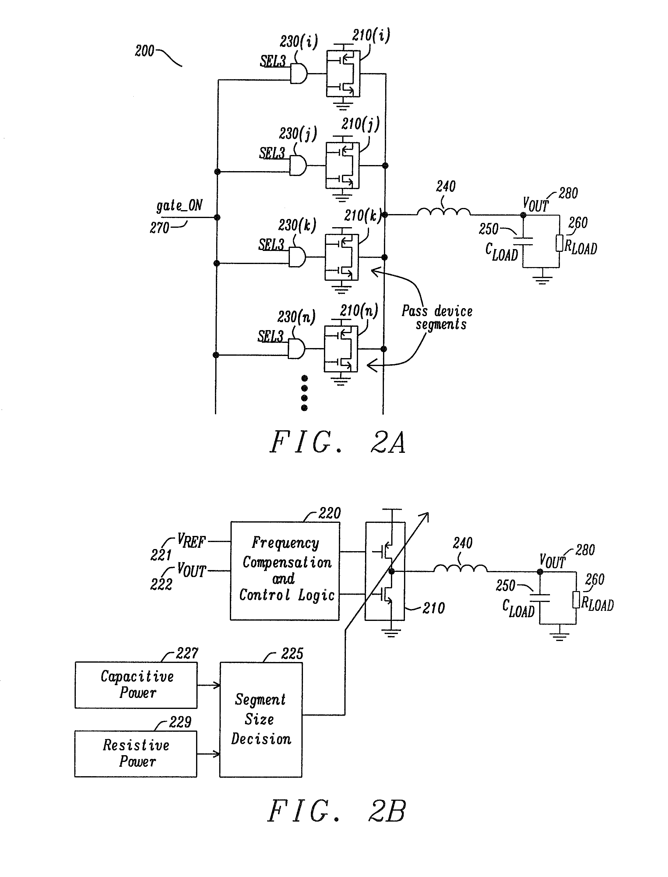
[0053]FIGS. 4A, 4B, and 4C are schematics of the components and ideal elements in accordance with the disclosure. FIGS. 4A, 4B and 4C includes the elements as enumerated,[0054]the current sense and slope ramp for Buck converter 410[0055]the Error amplifier and compensation network 420[0056]Buck SR_FF to generate duty cycle 430[0057]adaptive output stage pre-driver 440 and 445: SR_FF output is fed into 8 NAND gates which select the active PMOS driver transistors together with finger_sel decoder block (using nf) PMOS driver transistors 450, where the NMOS normally in the driver circuitry pull-down part of the driver is replaced with an ideal diode for simplicity, inductor and ideal current sense 460 output capacitor 470, average output current sense 480—here implemented by monitoring the inductor current and then through an RC filter, PMOS driver 490 voltage drop sense—implemented with ideal switches to sample ΔV when the transistor is ON, output of this block is Vsense of equation-7....
second embodiment
[0085]FIGS. 8A, 8B, and 8C a schematic 800 in accordance with a synchronous buck converter with a single comparators. FIGS. 8A, 8B, and 8C gives an embodiment with a single comparator where capacitive and resistive loss of both pass devices are compared together. The adaptive segment comprises of an NMOS and PMOS unit pass device. In this embodiment, the capacitive loss is calculated for each switching cycle for an adaptive segment as well as the resistive loss utilizing:
ΔV=D′×ΔVPMOS+D ΔVNMOS
or
ΔV=Isense×(D′×RPMOS+D×RNMOS)
[0086]FIGS. 8A, 8B, and 8C consists of the following blocks[0087](1) circuit block 810 and 820 whose output is cap_pow;[0088](2) the circuit block 830 and 835 where the circuit block 830 is a comparator which compares resistance power res_pow and capacitance power cap_pow;[0089](3) circuit block 840 configured to provide signal Vramp, and Vc_buck[0090](4) the comparator 850 whose inputs compare the input signal Vramp and the reference signal Vc_buck;[0091](5) RS fl...
PUM
 Abstract
Description
Claims
Application Information
PatSnap Eureka turns technology decisions into work you can execute. Powered by our Innovation Knowledge Graph, it runs expert workflows across engineering, life sciences, materials and intellectual property. Get your review-ready output in minutes.


