Transparent conductive films with embedded metal grids

a technology of transparent conductive films and embedded metal grids, which is applied in the direction of dielectric characteristics, conductive layers on insulating supports, instruments, etc., can solve the problems of high manufacturing cost, limited suitability for many applications, and reach the stage of being fully commercialized, so as to improve mechanical strength and stability, cost-effective

Active Publication Date: 2016-11-24
VERSITECH LTD
View PDF5 Cites 27 Cited by
  • Summary
  • Abstract
  • Description
  • Claims
  • Application Information

AI Technical Summary

Benefits of technology

[0004]Embodiments of the present invention pertain to novel metal mesh based flexible transparent conductive film structures with a metal mesh embedded in a substrate and methods of fabrication thereof. The metal mesh may have a cap that is pressed and embedded in a substrate or a deformable material on a substrate. Therefore, when the substrate is bent, the cap helps anchor the metal mesh in the substrate, keeping the metal mesh securely fastened and helping to improve its mechanical strength and stability. In one embodiment, the surface of the metal mesh is flush with the substrate surface. The resulting transparent conductive electrode (TCE) may then have a smooth surface, which is important for device integration.
[0005]According to another embodiment of the present invention, a cost-effective approach for fabricating a metal mesh TCE involving lithography, electroplating, and thermal imprint transfer is also provided. Such fabrication methods allow for large-volume production of TCEs at a low cost.

Problems solved by technology

However, for many industrial applications, conventional materials have problems such as film brittleness, low infrared transmittance, and low abundance, limiting their suitability for many applications.
Graphene and carbon nanotube based TCEs are being studied in research labs, but have yet to reach the stage of being fully commercialized.
However, their high manufacturing cost and complicated manufacturing process have hindered the development and application of metal grid TCEs.

Method used


Image

  • Transparent conductive films with embedded metal grids
  • Transparent conductive films with embedded metal grids
  • Transparent conductive films with embedded metal grids

Examples


example 1

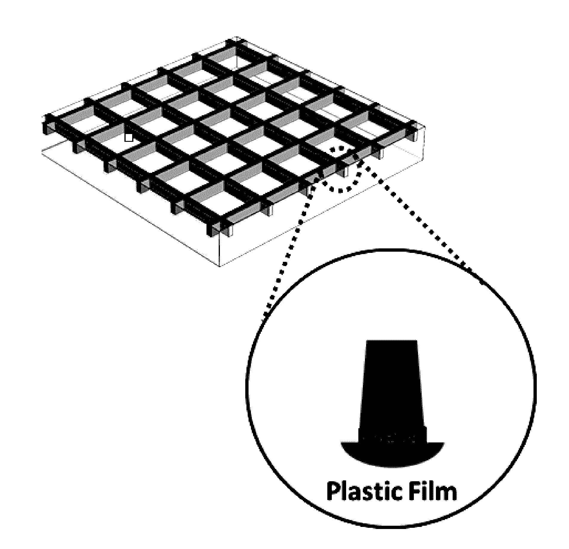
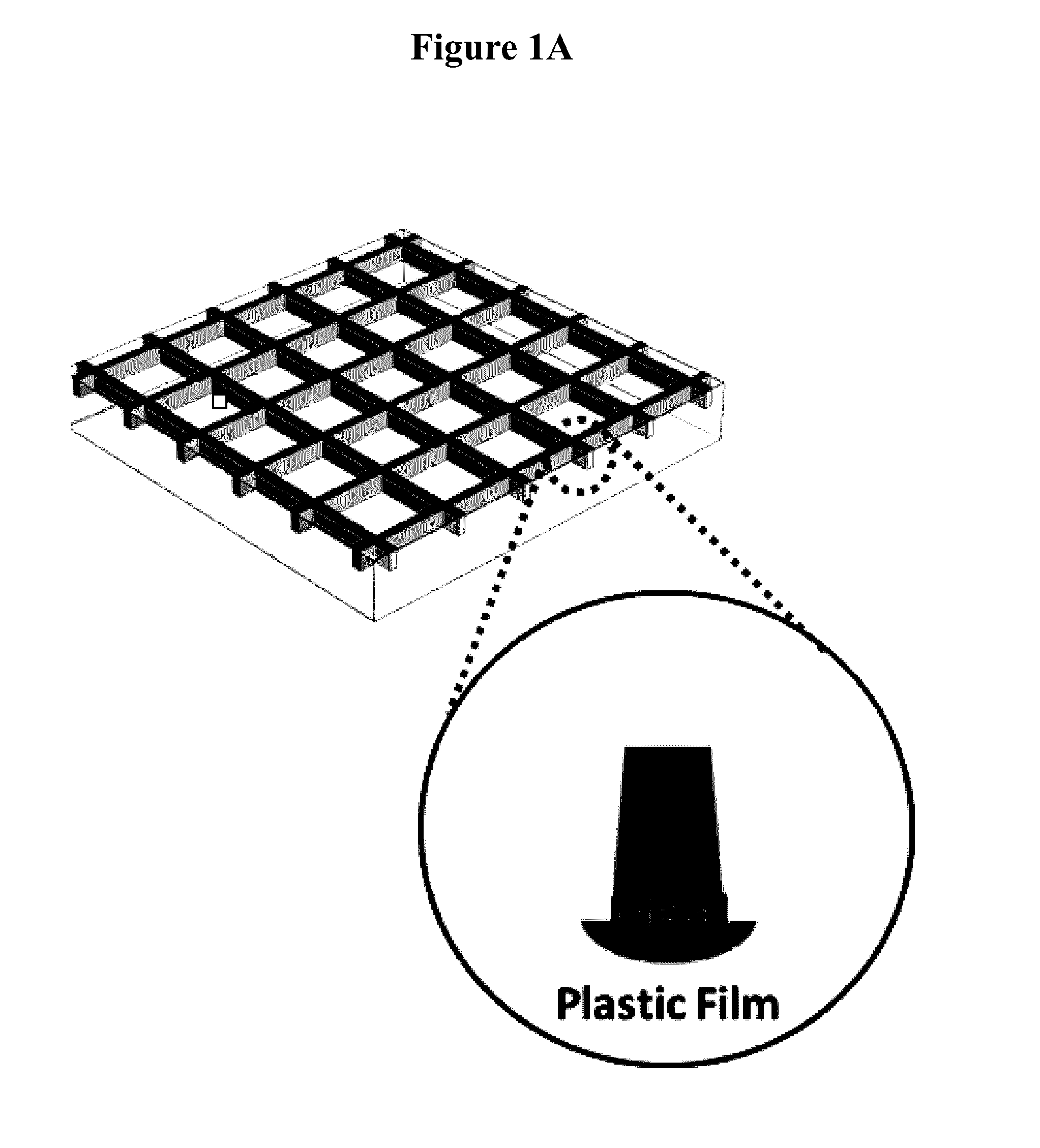
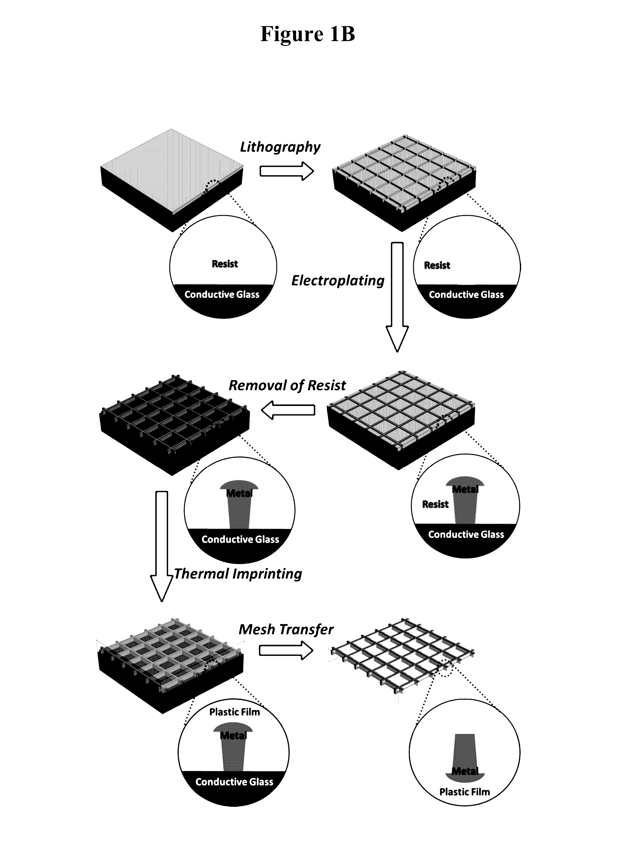
[0034]An embodiment of the present invention was fabricated as seen in FIGS. 4A-C. In the TCE structure embodiment of FIGS. 4A-C, a Cu mesh TCE was fabricated using the above stated fabrication procedure with photolithography being used to pattern the resist. FIG. 4A shows a grid pattern in the resist after the resist was first exposed during photolithography using a grid pattern and then developed. SEM and AFM characterizations show that the lithography patterned resist had a linewidth of about 4 microns and a depth of about 2 microns. The openings in the grid were about 50 microns. After electroplating copper into the grid trenches and removing the resist, the copper grid was obtained on a conductive substrate, such as an FTO glass substrate, as shown in FIG. 4B. Then, a thermoplastic film such as a cyclic olefin copolymer film was placed on the metal grid, heated, and then pressed. That is, the metal grid was pressed into the softened plastic film. After cooling and peeling off t...

example 2

[0035]A fabrication method according to an embodiment of the present invention was used to form a sub-micron metal grid as shown in FIGS. 5A-5C, where a copper metal grid with 0.8 micron linewidths and 10 micron openings was fabricated. FIGS. 5A, 5B and 5C each illustrates the SEM and AFM results during this fabrication at different stages. Specifically, FIG. 5A shows the grid pattern in the resist after the lithography step, FIG. 5B shows the copper grid on the conductive substrate after electroplating and resist removal steps, and FIG. 5C shows the final copper grid TCE with the copper grid transferred and embedded in a plastic film to form a flexible transparent electrode.

example 3

[0036]In order to incorporate a metal grid TCE into device applications, a large-area TCE according to an embodiment of the present invention was fabricated, as seen in FIG. 6. The TCE of FIG. 6 had a large-area (5 cm×5 cm) copper grid TCE with >90% transmittance and 0.93 ohm / sq sheet resistance. A large-area TCE with a size of 5 cm by 5 cm is sufficient for lighting devices, display devices, and touchscreen devices. Large sizes are achievable by: 1) fabricating small metal grids on conductive substrates (such as FTO glass) and then stitching them together to form a large plastic substrate by a step and repeat pressing process; or 2) using a large-area conductive substrate to directly fabricate a large-area metal grid TCE.


PUM

PropertyMeasurementUnit
heightaaaaaaaaaa
depthaaaaaaaaaa
depthaaaaaaaaaa

Abstract

A transparent conductive film with a metal mesh embedded in a substrate and a method of fabrication thereof is provided. The metal mesh has a cap that is pressed and embedded in a substrate or a deformable material on a substrate, providing superior mechanical stability by mechanical interlocking. The embedding mechanism also provides superior chemical and environmental stability. A fabrication method is provided and includes a vacuum-free and low-cost process for large-volume manufacturing of the transparent conductive film with tunable performance.

Description

CROSS-REFERENCE TO RELATED APPLICATION[0001]This application claims the benefit of U.S. provisional application Ser. No. 62 / 165,566, filed May 22, 2015, which is herein incorporated by reference in its entirety.BACKGROUND OF THE INVENTION[0002]The present invention relates to the field of transparent conductive electrodes (TCEs) and films. Conventional materials for TCEs include thin films of transparent oxides (TCOs), which have reasonable electronic performance. However, for many industrial applications, conventional materials have problems such as film brittleness, low infrared transmittance, and low abundance, limiting their suitability for many applications. To overcome these limitations, several new generation TCEs based on graphene, carbon nanotubes, metal nanowire networks, and metal mesh are proposed.[0003]Silver nanowire based TCEs are often used in touch screen products. Graphene and carbon nanotube based TCEs are being studied in research labs, but have yet to reach the ...

Claims


Application Information

Patent Timeline
Patent Type & Authority Applications(United States)
IPC IPC(8): H05K1/02C25D5/48H05K1/03C25D7/00H05K3/18H05K3/46C25D5/02C25D5/54
CPCH05K1/0274C25D5/022C25D5/48C25D5/54C25D7/00H05K2201/0108H05K1/028H05K3/188H05K3/4611H05K1/0306H05K1/0296C25D1/04C25D1/08G06F2203/04103G06F2203/04112H01B1/02H01B5/14H01B13/0026H01L21/0273H01L21/288
Inventor KHAN, ARSHADLI, WENDI
Owner VERSITECH LTD
Why Eureka
Try Eureka