

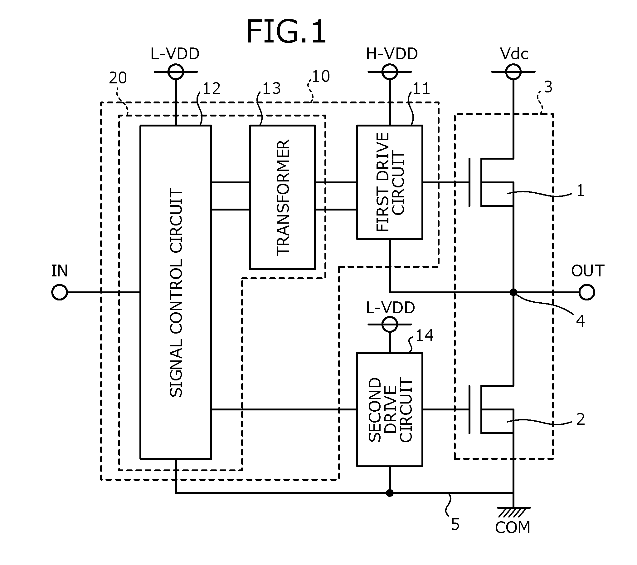
Isolator and method of manufacturing isolator
a manufacturing method and isolation technology, applied in the direction of transformer/inductance details, fixed transformers or mutual inductances, inductances, etc., can solve the problems of difficult to reduce the size of signal processing systems equipped with these isolators, high cost and high power consumption of transformers, etc., to achieve high noise resistance, high cost, and high insulation resistan
- Summary
- Abstract
- Description
- Claims
- Application Information
AI Technical Summary
Benefits of technology
Problems solved by technology
Method used
Image

Examples
first embodiment
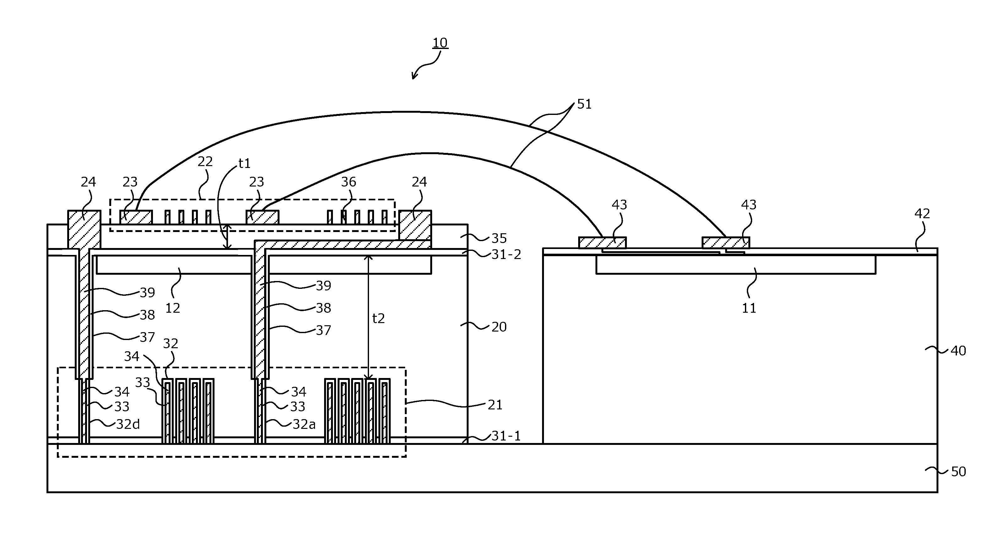
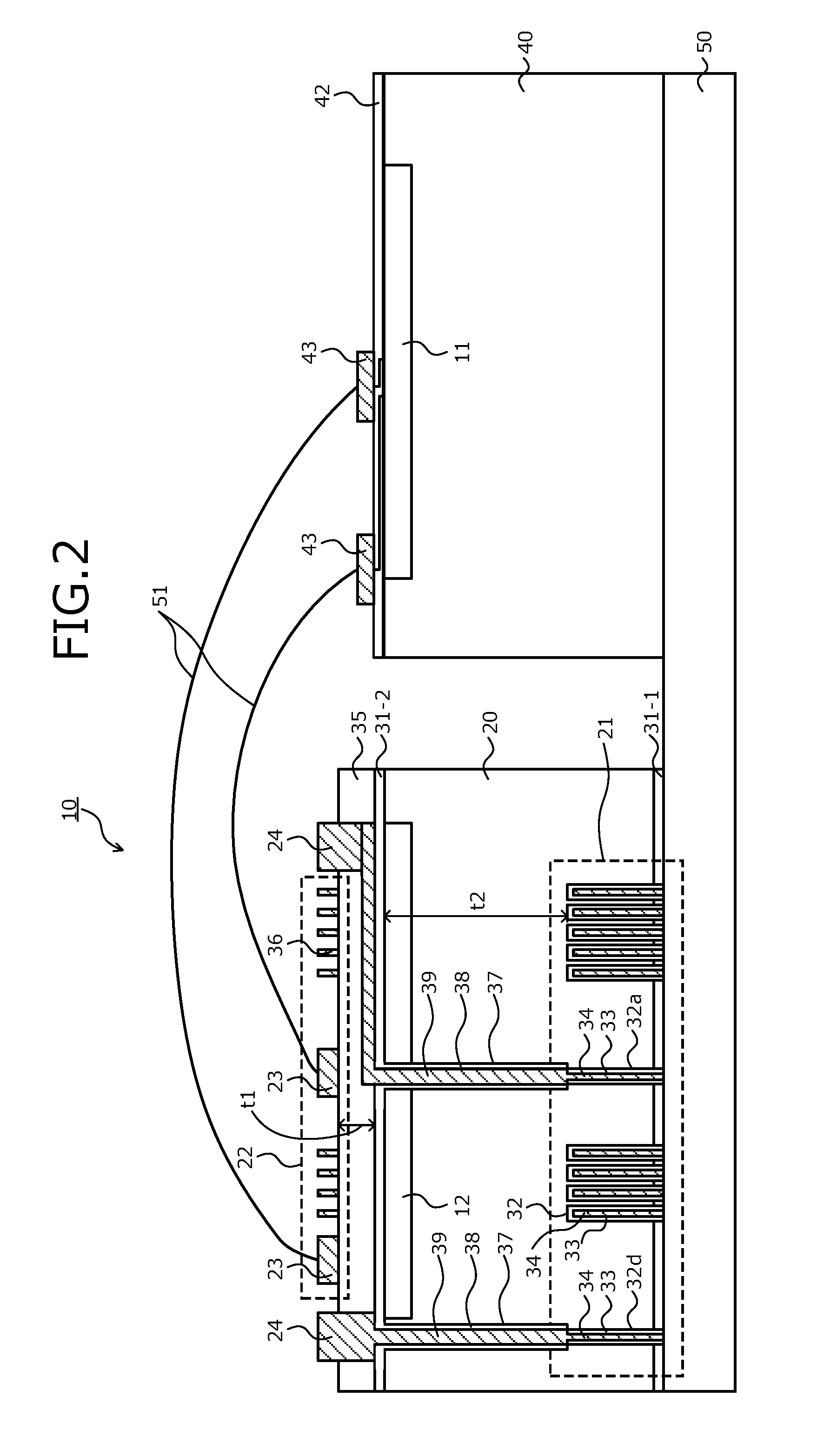
[0090]A position of the transmission circuit 12 along a direction (horizontal direction) parallel to the substrate front surface will be described. FIGS. 13 to 15 are schematic plan views of the horizontal position of the transmission circuit disposed on the isolator according to the FIGS. 13 to 15 depict the horizontal position of the transmission circuit 12 relative to the first coil 21. FIGS. 13 to 15 depict only the first coil 21 among the first and second coils 21 and 22 configuring the transformer 13. As depicted in FIG. 13, the transmission circuit 12 may be disposed such that the transmission circuit 12 almost entirely overlaps the first coil 21 in the depth direction. In this case, the chip size may be reduced to a size that barely encompasses the outermost perimeters of the first coil 21 and the second coil 22.
[0091]The center of the spiral of the coil (the position of the inner end portion 21a of the first coil 21) has the highest magnetic field strength (magnetic flux d...
second embodiment
[0096] since the first coil (secondary-side coil) and the second coil (primary-side coil) are formed on the back surface side and the front surface side, respectively, of the first semiconductor substrate, the coils do not oppose each other on the trench side wall surfaces as in the case of a conventional transformer having respective coils formed within two trenches. Therefore, the area of the opposing portions of the primary-side coil and the secondary-side coil may be made smaller as compared to a conventional transformer, and the parasitic capacitance between the coils may be reduced. As a result, the delay time of signal transfer from the transmission circuit to the reception circuit may be shortened and the electrical characteristics of the isolator may be improved. By changing the thickness of the first semiconductor substrate, the depth of the coil trench, and the thickness of the insulating layer on the substrate front surface, the thickness of the portion between the prima...
third embodiment
[0100]FIG. 18 is a schematic cross-sectional view of a portion of another example of a semiconductor apparatus to which the isolator is applied. As depicted in FIG. 18, the second semiconductor substrate 40 may be disposed with the front surface facing downward on the first semiconductor substrate 20. In this case, bump electrodes 48 are disposed on the third electrode pads 43 of the front surface of the second semiconductor substrate 40. The second semiconductor substrate 40 is placed with the front surface facing downward on the front surface of the first semiconductor substrate 20. The bump electrodes 48 of the second semiconductor substrate 40 are joined to the first electrode pads 23 exposed on the front surface of the first semiconductor substrate 20. When the second semiconductor substrate 40 is disposed with the front surface facing downward on the first semiconductor substrate 20, the electrode portions of the reception circuit 11 may be led out to the substrate back surfa...
PUM
 Abstract
Description
Claims
Application Information