
Semiconductor device and semiconductor device manufacturing method

Active Publication Date: 2017-02-02
FUJI ELECTRIC CO LTD
View PDF10 Cites 1 Cited by
  • Summary
  • Abstract
  • Description
  • Claims
  • Application Information

AI Technical Summary

Benefits of technology

This patent is for a semiconductor device and manufacturing method that aims to achieve better trade-offs between on-state voltage and switching loss while maintaining breakdown resistance and preventing the rise in threshold voltage and on-state voltage. The invention prevents an increase in the width of the lower end of a semiconductor region during thermal processing, which helps to decrease breakdown resistance. Additionally, the invention prevents encroachment of another semiconductor region into a channel portion, which helps to maintain the width of the third semiconductor region and prevents the rise in threshold voltage. Overall, this invention allows for the miniaturization of a trench gate semiconductor device while maintaining good trade-offs between on-state voltage and switching loss.

Problems solved by technology

Therefore, there is a problem in that short-circuit resistance and latch-up resistance (hereafter referred to collectively as breakdown resistance) decreases.
Also, as well as low on-state voltage, high speed switching characteristics are also required of a power semiconductor device, because of which improvement of high speed switching characteristics (a reduction of switching loss Eoff), which are in a trade-off relationship with the low on-state voltage Von, is also an important problem.

Method used


Image

  • Semiconductor device and semiconductor device manufacturing method
  • Semiconductor device and semiconductor device manufacturing method
  • Semiconductor device and semiconductor device manufacturing method

Examples


first embodiment

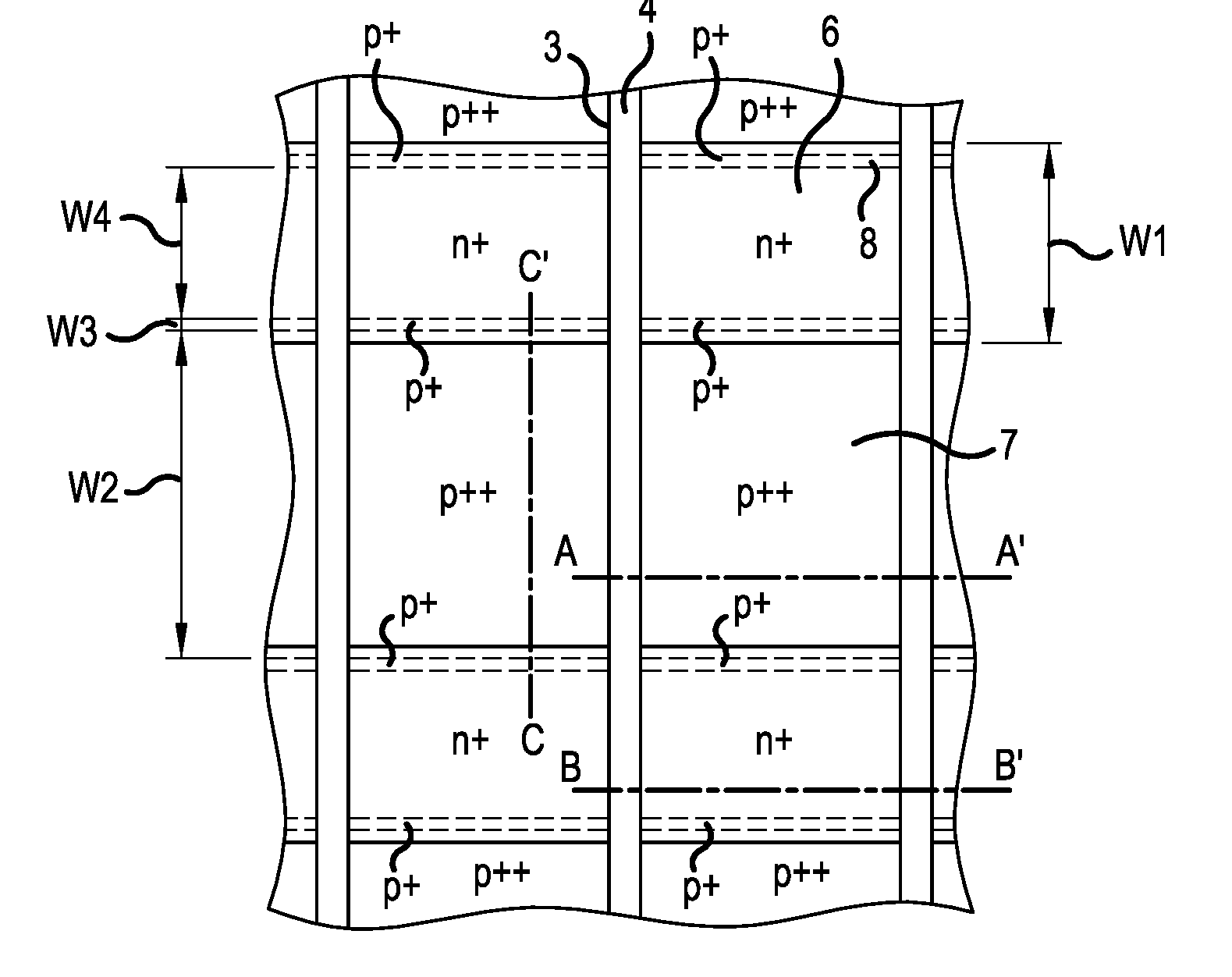
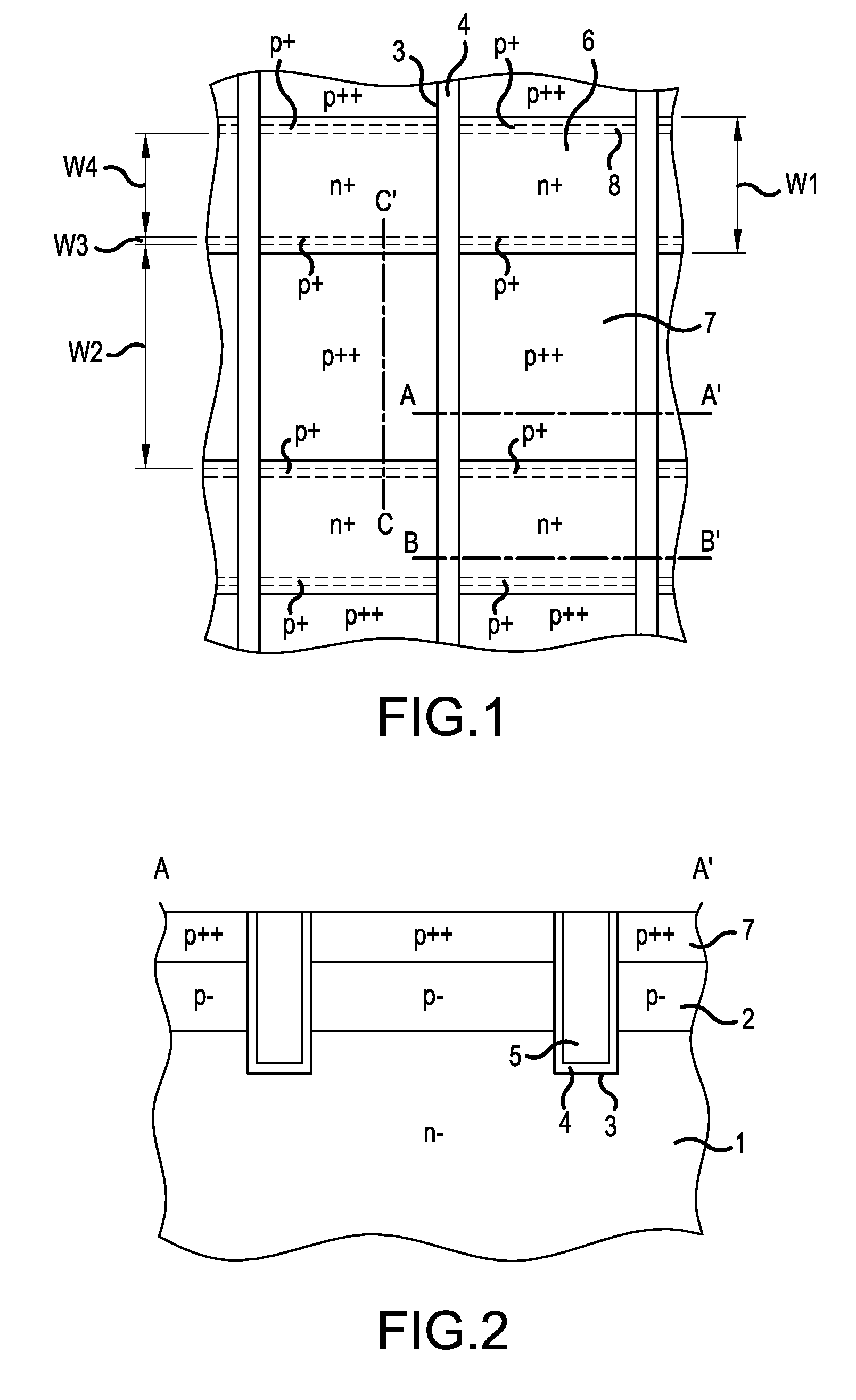
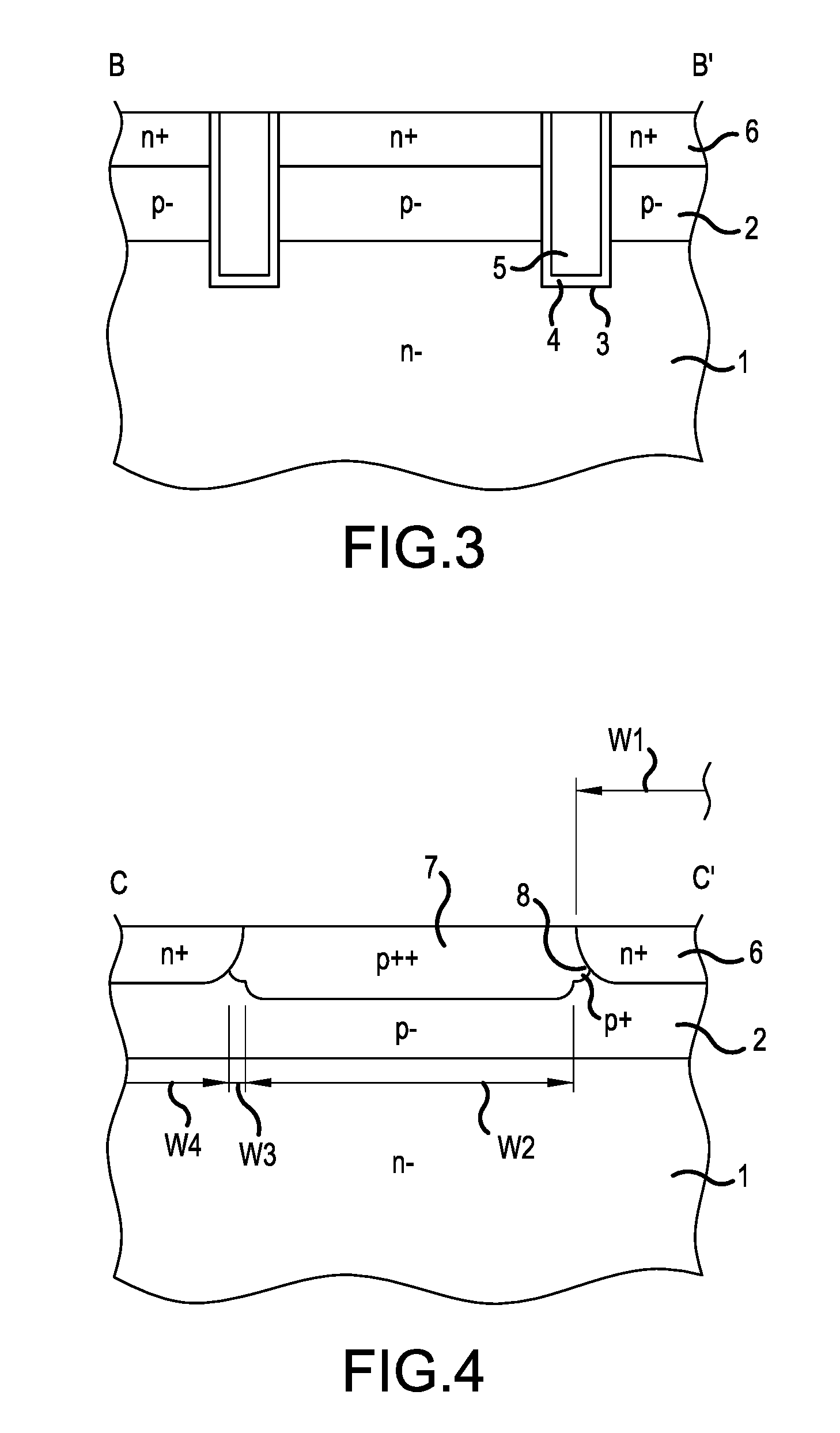
[0056]A description will be given of the structure of a semiconductor device according to a first embodiment. FIG. 1 is a plan view showing the planar layout of a trench gate structure of the semiconductor device according to the first embodiment. A gate dielectric, interlayer dielectric, source electrode, and passivation film are omitted from FIG. 1 (the same applies to FIGS. 2 to 4, 10, and 14). FIG. 2 is a sectional view showing the sectional structure along a section line A-A′ of FIG. 1. FIG. 3 is a sectional view showing the sectional structure along a section line B-B′ of FIG. 1. FIG. 4 is a sectional view showing the sectional structure along a section line C-C′ of FIG. 1. The section line A-A′ passes through a trench 3 and a p++-type contact region (fourth semiconductor region) 7. The section line B-B′ passes through the trench 3 and an n+-type emitter region (third semiconductor region) 6. The section line C-C′ passes through the n+-type emitter region 6, the p++-type conta...

second embodiment

[0082]A description will be given of the structure of a semiconductor device according to a second embodiment. FIG. 10 is a sectional view showing main portions of a trench gate structure of the semiconductor device according to the second embodiment. FIG. 10 shows the sectional structure along the section line C-C′ of FIG. 1. The planar layout of the trench gate structure, the sectional structure passing through the trench 3 and p++-type contact region 7 (the section line A-A′ of FIG. 1), and the sectional structure passing through the trench 3 and n+-type emitter region 6 (the section line B-B′ of FIG. 1) are the same as in the first embodiment (refer to FIGS. 1 to 3). The semiconductor device according to the second embodiment differs from the semiconductor device according to the first embodiment in that the depth of a p+-type region 28 that covers an end portion on the lower side of the junction interface between the n+-type emitter region 6 and p++-type contact region 7 is gre...

third embodiment

[0089]A description will be given of the structure of a semiconductor device according to a third embodiment. FIG. 14 is a perspective view showing main portions of a trench gate structure of the semiconductor device according to the third embodiment. The semiconductor device according to the third embodiment differs from the semiconductor device according to the first embodiment in that a mesa portion configured as a unit cell structure by providing the n+-type emitter region 6, and a mesa portion configured as a p−-type floating region 42 without providing the n+-type emitter region 6, are disposed in the p−-type base region 2 sandwiched by neighboring trenches 3. Specifically, a mesa portion configured as a unit cell formed of the n+-type emitter region 6 and p++-type contact region 7 and a mesa portion configured as the p−-type floating region 42, which has emitter potential, are repeatedly alternately disposed in the second direction perpendicular to the first direction, in whi...


PUM


Abstract

A semiconductor device and manufacturing method achieve miniaturization, prevent rise in threshold voltage and on-state voltage, and prevent decrease in breakdown resistance. N+-type emitter region and p++-type contact region are repeatedly alternately disposed in a first direction in which a trench extends in stripe form in a mesa portion sandwiched between trench gates. P+-type region covers an end portion on lower side of junction interface between n+-type emitter region and p++-type contact region. Formation of trench gate structure is such that n+-type emitter region is selectively formed at predetermined intervals in the first direction in the mesa portion by first ion implantation. P+-type region is formed less deeply than n+-type emitter region in the entire mesa portion by second ion implantation. The p++-type contact region is selectively formed inside the p+-type region by third ion implantation. N+-type emitter region and p++-type contact region are diffused and brought into contact.

Description

BACKGROUND OF THE INVENTION[0001]A. Field of the Invention[0002]The present invention relates to a semiconductor device and semiconductor device manufacturing method.[0003]B. Description of the Related Art[0004]To date, insulated gate bipolar transistors (IGBTs) have been in the public domain as power semiconductor devices used in industrial machines and automobiles, domestic electrical appliances, and the like. Among power semiconductor devices, IGBTs in particular have good gate control, and can achieve low on-state voltage owing to a conductivity modulation effect. Also, two kinds of structure are widely known as MOS gate (an insulated gate formed of metal-oxide-semiconductor) structures of a power semiconductor device, those being a planar gate structure wherein a MOS gate is provided in plate form on a semiconductor substrate, and a trench gate structure wherein a MOS gate is embedded inside a trench formed in a semiconductor substrate.[0005]The trench gate structure can be pro...

Claims


Application Information

Patent Timeline
IPC IPC(8): H01L29/739H01L21/266H01L29/66H01L29/08H01L29/10H01L21/265H01L29/06
CPCH01L29/7397H01L21/26513H01L21/266H01L29/0615H01L29/66348H01L29/1004H01L29/0696H01L29/1087H01L29/0804H01L29/0603H01L29/083H01L29/0821
Inventor NAITO, TATSUYA
Owner FUJI ELECTRIC CO LTD
Learn More